
Study on Charge Carriers Behavior at CdS/TiO2 Interface of One Dimensional TiO2@CdS Core-shell Structure by Raman Scattering and Surface Photovoltage Spectroscopy
Received date: 2012-10-22
Online published: 2013-02-21
Supported by
Project supported by the the National Natural Science Foundation of China (No. 20903038), the Supporting Project for Young Teacher of Hunan University,the Best Youth of The Education Department Of Hunan Province (No. 11B012).
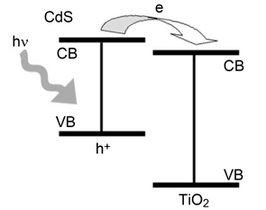
TiO2 nanowires with the diameter of about 90 nm and length of dozens of micron meter were synthesized by thermal annealing of Ti foil under the catalysis of Pd nanoparticles which were deposited on Ti foil with the ultraviolet light photoreduction. CdS shell grew on the surface of TiO2 nanowires by chemical bath deposition (CBD) to form the 1D TiO2@CdS core/shell nanostructures. The thickness of CdS shell was controlled by varying the concentration of the citric acid. The scanning electron microscope (SEM) and transmission electron microscope (TEM) characterization implied that CdS shell thickness on TiO2 nanowire were about 20, 30 and 60 nm, synthesized in the solutions with citric acid concentration of 0.095, 0.19 and 0.38 mmol/L, respectively. The Raman scattering of pure TiO2 nanowire and TiO2@CdS core/shell structures excited by 488 nm Argon ion laser indicates that the modification of CdS on TiO2 nanowire with proper thickness (20 to 30 nm) can increase both the Raman scattering resulted from CdS and TiO2. It is attributed to the photo-induced electron transfering from CdS shell and TiO2 core, which results in the quenching of fluorescence of CdS, and the increase of electron distribution density for TiO2 excited state. The surface photovoltage (SPV) spectrum characterization, based on the separation of photo-generated electron-hole in space, agrees well with the Raman scattering results. That is, TiO2@CdS core/shell structures with 30 nm CdS have highest SPV response intensity and broadest spectrum range, due to the effective charge transfer between CdS and TiO2. The systematic study about the dependence of the Raman scattering and SPV on the CdS shell thickness demonstrated that the diffusion length of electron in CdS shell is between 30 and 60 nm, and it is optimal for one-dimension TiO2@CdS nanostructures in optoelectric devices application with the CdS shell thickness thinner than light penetration depth and electron diffusion length in CdS.
Zhang Qinglin , Cao Shangcao , Xia Mingxia , Wang Xiaojian , Wan Qiang , Pan Anlian . Study on Charge Carriers Behavior at CdS/TiO2 Interface of One Dimensional TiO2@CdS Core-shell Structure by Raman Scattering and Surface Photovoltage Spectroscopy[J]. Acta Chimica Sinica, 2013 , 71(04) : 634 -638 . DOI: 10.6023/A12100810
/
| 〈 |
|
〉 |
