


1 引言
2 超浸润界面与液桥形成调控
2.1 界面浸润性
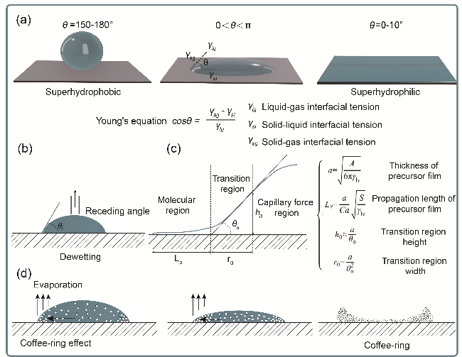
图1 液体的宏观退浸润行为. (a)表面浸润性与杨氏方程. (b)接触角滞后性示意图. (c)液体三相接触线附近的动力学模型. (d)咖啡环效应的形成过程Figure 1 Interfacial wettability and dewetting behavior. (a) Surface wettability and Young’s equation. (b) Schematic illustration of contact angle hysteresis. (c) Dynamic model near the three-phase contact line. (d) Formation process of the coffee-ring effect |
2.2 液体退浸润过程
2.3 液桥的形成与调控

图2 液桥的形成机制. (a)拉普拉斯压力差驱动液桥形成. (b)特殊模板诱导产生的储液区与液桥形成过程. (c)特殊液桥结构的荧光显微镜图像. (d) 4英寸晶圆上实现的高均匀性结构[35]Figure 2 Mechanism of Liquid Bridge Formation. (a) Formation of liquid bridges driven by Laplace pressure difference. (b) Reservoir area formation and liquid bridge generation induced by special templates. (c) Fluorescence microscopy image of a special liquid bridge structure. (d) High-uniformity structure achieved on a 4-inch wafer.[35] Copyright 2021, Springer Nature |
3 液桥限域组装机理
3.1 液桥退浸润过程中三相接触线的锚定与滑移

图3 液桥限域组装机理. (a)三相接触线附近的受力分析. (b)不同弯液面直径Dm的液桥退浸润过程荧光图像. (c)退浸润过程中组装动力学与Dm的关系[37]. (d)三相接触线的锚定与移动诱导组装单元形成长程有序结构[39]. (e)三相接触线附近的组装过程模拟[38]Figure 3 Mechanism of confined assembly via liquid bridges. (a) Force analysis near the three-phase contact line. (b) Fluorescence images of dewetting liquid bridges with different meniscus diameters (Dm). (c) Relationship between assembly dynamics and Dm during the dewetting process[37]. Copyright 2022, Wiley-VCH. (d) Formation of long-range ordered structures induced by pinning and movement of the three-phase contact line[39]. Copyright 2018, Wiley-VCH. (e) Simulation of the assembly process near the three-phase contact line[38]. Copyright 2022, Wiley-VCH |
3.2 液桥限域组装机理的普适性

图4 液桥限域组装技术的普适性分析. (a)液桥的影响因素与半定量的普适性公式[39]. (b)液桥限域组装技术在不同尺度材料下的普适性[39,40-42].Figure 4 Universality analysis of liquid-bridge-confined assembly. (a) Influencing factors of liquid bridges and a semi-quantitative universal formula[39]. Copyright 2018, Wiley-VCH. (b) Universality of the liquid bridge confined assembly technique across materials of different scales[39,40-42]. Copyright 2018, 2022, Wiley-VCH |
4 长程有序结构对器件光电性能的影响
4.1 有序的π-π堆积

图5 长程有序结构对材料光电性质的影响. (a)有序的π-π重叠[43]. (b)电子带状传输[44]. (c)电子离域增强[45]. (d)尺寸依赖的光电性能优化[53]Figure 5 Effects of long-range ordered structures on the optoelectronic properties of materials. (a) Ordered π-π stacking[43]. Copyright 2024, Wiley-VCH. (b) Band-like electron transport[44]. Copyright 2019, Springer Nature. (c) Enhanced electron delocalization[45]. Copyright 2023, Wiley-VCH. (d) Optimization of size-dependent photoelectric properties[53]. Copyright 2018, Springer Nature |
4.2 带状电子传输
4.3 电荷离域与超晶格耦合
4.4 尺寸依赖的光电性能优化
5 液桥限域长程有序组装结构的光电应用
5.1 微激光器与激光-波导耦合

图6 微型激光器. (a)有机纳米线阵列的荧光显微图像与透射电子显微镜图像. (b)长度分别为20、50和70 mm的纳米线的荧光显微图像、电场分布模拟结果及激光发射光谱[57]. (c)毛细管桥组装系统的退浸润过程示意图(上)与荧光显微镜图像(下). (d)光密码学基元认证原理示意图. (e)不同激光发射的腔长分布统计. (f) 64×16位四元随机比特阵列[58]. (g)调控不同界面浸润性实现分级限域组装过程的原理示意图. (h)多组分红绿蓝(RGB)量子点微环阵列的荧光显微图像及对应的原子力显微镜图像与扫描电子显微镜图像. (i) R, G, B量子点激光像素的光致发光(PL)光谱[59]Figure 6 Micro laser devices. (a) Fluorescence microscopy image and transmission electron microscopy image of organic nanowire arrays. (b) Fluorescence microscopy images, electric field distribution simulation results, and laser emission spectra of nanowires with lengths of 20, 50, and 70 mm[57]. Copyright 2020, Elsevier. (c) Schematic of the dewetting process in the capillary-bridge assembly system (top) and corresponding fluorescence microscopy image (bottom). (d) Schematic of the authentication principle for cryptographic primitives. (e) Statistical distribution of cavity lengths for different laser emissions. (f) 64×16 quaternary random bit array[58]. Copyright 2019, Wiley-VCH. (g) Schematic of the hierarchical confined assembly process achieved by controlling different interface wettabilities. (h) Fluorescence microscopy image of multicomponent red-green-blue (RGB) quantum dot microring arrays, along with corresponding atomic force microscopy and scanning electron microscopy images. (i) Photoluminescence (PL) spectra of R, G, and B quantum dot laser pixels[59]. Copyright 2024, Wiley-VCH |

图7 激光-波导耦合结构. (a)液桥中静电外延机制定向调控钙钛矿成核与生长机制. (b)耦合双微线的阈值上空间分辨PL光谱. (c)阈值上的耦合双微线条的荧光显微图像与实空间PL图像(左)和归一化PL光谱(右), 各对应位置激光模式能量匹配[64]. (d)微环-波导耦合组装结构示意图. (e)荧光显微图像, 扫描电子显微镜图像与有限元模拟对比的微环与波导结构. (f)对应光谱数据显示微环激光发射峰与波导激光发射峰. (g)微环激光器激发与输出场景的对应关系(左), 四个输出场景的荧光显微图像(右). (h)基于ASCII编码的概念验证, 将光信号组合转换为字符[37]Figure 7 Laser-waveguide coupling structures. (a) Electrostatic epitaxy mechanism in the liquid bridge for oriented control of perovskite nucleation and growth. (b) Spatially resolved PL spectra at the lasing threshold of coupled dual microwires. (c) Fluorescence microscopy image and real-space PL image (left), and normalized PL spectra (right) of coupled microwires at threshold, showing mode energy matching at specific positions[64]. Copyright 2023, Wiley-VCH. (d) Schematic of the micro-ring-waveguide coupled assembly. (e) Fluorescence microscopy, SEM image, and finite element simulation of the micro-ring and waveguide structure. (f) Corresponding spectral data showing lasing peaks from both the micro-ring and waveguide. (g) Correlation between micro-ring laser excitation and output states (left), with fluorescence images of four output conditions (right). (h) Conceptual demonstration of ASCII encoding by converting combinations of optical signals into characters[37]. Copyright 2022, Springer Nature |
5.2 发光二极管

图8 发光二极管. (a)微柱模板的抗粘附改性处理. (b) InP基绿色量子点薄膜扫描电镜图像. (c) QLED器件结构示意图. (d) InP基红色QLED大面积器件及其电流密度-亮度-电压特性曲线和外量子效率-电流效率-亮度特性曲线[70]. (e)分层限域组装工艺示意, 通过正交方向沉积构建交叉像素阵列. (f)不同CBP-V含量下交联处理的蓝色量子点薄膜光致发光保留率随时间变化曲线. (g) RGB量子点像素单元荧光显微图像. (h)全彩色QLED器件结构. (i)器件工作状态下的外量子效率-亮度特性曲线与不同驱动电压下的电致发光(PL)图谱. (j)器件在CIE色度图中的坐标分布[68]Figure 8 Light-emitting diodes. (a) Anti-adhesion modification of micropillar templates. (b) SEM image of InP-based green quantum dot film. (c) Schematic of the QLED device structure. (d) Large-area InP-based red QLED device and its current density-luminance-voltage and EQE-current efficiency-luminance characteristics[70]. Copyright 2025, Springer Nature. (e) Schematic of layered confined assembly for cross pixel array construction via orthogonal deposition. (f) Time-dependent photoluminescence retention of blue quantum dot films with different CBP-V contents after crosslinking. (g) Fluorescence microscopy image of RGB quantum dot pixel units. (h) Structure of the full-color QLED device. (i) EQE-luminance characteristics and EL (PL) spectra under varying driving voltages. (j) CIE chromaticity coordinate distribution of the devices[68]. Copyright 2025, American Chemical Society |
5.3 偏振探测与方位识别

图9 偏振光电探测器件. (a)偏振响应微线器件示意图. (b)微线内长程有序高取向性结构的高分辨率扫描电镜特写. (c)组装微线器件在不同光强下的I-V特性曲线[39]. (d)集成线偏振与圆偏振光探测的多功能光电探测器示意图与纳米线的掠入射广角X射线散射图谱. (e)不同斯托克斯参量对应的光偏振态与理论吸收值的偏振依赖性. (f)不同偏振光下的实验测量值与理论值对比[76]. (g)垂直亚波长钙钛矿纳米线阵列的扫描电镜图像. (h)用于检测三维空间光入射方向的垂直钙钛矿纳米线结构与对应的模拟结果极坐标图. (i)基于同一水平面上相距5 cm的两个垂直角度传感装置的光源空间定位示意图[70]Figure 9 Polarized optoelectronic detector devices. (a) Schematic of a polarization-responsive microwire device. (b) High-resolution SEM close-up of highly oriented, long-range ordered structures inside the microwire. (c) I-V curves of the assembled microwire device under varying light intensities[39]. Copyright 2022, Wiley-VCH. (d) Schematic of a multifunctional optoelectronic detector integrating linear and circular polarization detection, along with the grazing-incidence wide-angle X-ray scattering (GIWAXS) pattern of nanowires. (e) Polarization dependence of theoretical absorption corresponding to different Stokes parameters. (f) Comparison of experimental and theoretical values under different polarization states[76]. Copyright 2021, American Chemical Society. (g) SEM image of vertically aligned subwavelength perovskite nanowire arrays. (h) Polar plot of simulated results for vertical perovskite nanowire structures designed to detect 3D light incidence directions. (i) Schematic of spatial light source localization using two angular sensors placed 5 cm apart on the same horizontal plane[70]. Copyright 2025, American Chemical Society |
5.4 柔性可穿戴器件

图10 柔性与可穿戴器件. (a)基于DTT-8一维阵列器件的光学图像、局部放大的扫描电子显微镜图像和有机单晶微米线阵列的GIWAXS图谱. (b)多次弯曲循环测试下的器件迁移率变化. (c)不同光照功率下的电流-时间响应特性. (d)可穿戴紫外线监测手环结构示意. (e)实际适用场景中手环在紫外光照下的响应效果[43]. (f)基于曲线微结构阵列的全可拉伸器件结构示意图与112个全可拉伸器件阵列的光学图像. (g)弯曲P3HT微结构阵列的GIWAXS图谱. (h)与非门在0%和100%应变下的输入-输出特性曲线. (i)可拉伸的与非门在初始状态和沿电荷传输方向水平方向施加100%应变下的光学图像(VA/VB为A/B端输入电压). (j)器件在未拉伸状态和沿电荷传输方向平行/垂直施加100%应变时的转移特性曲线. (k)器件在50%应变下经历1000次拉伸-释放循环的迁移率统计[35]Figure 10 Flexible and wearable devices. (a) Optical image of the DTT-8 1D array-based device, magnified SEM image, and GIWAXS pattern of organic single-crystal microwire arrays. (b) Mobility variation of the device under multiple bending cycles. (c) Current-time response characteristics under different illumination powers. (d) Schematic of a wearable UV monitoring wristband. (e) UV response performance of the wristband under real-world conditions[43]. Copyright 2024, Wiley-VCH. (f) Schematic and optical image of a fully stretchable device structure based on curved microstructure arrays with a 112-device array. (g) GIWAXS pattern of the bent P3HT microstructure arrays. (h) Input-output characteristics of an AND-NOT gate under 0% and 100% strain. (i) Optical image of the stretchable AND-NOT gate in the initial state and under 100% strain applied horizontally along the charge transport direction (VA/VB are input voltages at terminals A/B). (j) Transfer characteristics of the device in the unstretched state and under 100% strain applied parallel/perpendicular to the charge transport direction. (k) Statistical mobility data after 1000 stretch-release cycles under 50% strain[35]. Copyright 2021, Springer Nature |