

1 引言
目前工业上常用的H2提纯方法主要依赖于低温精馏、冷凝、变压吸附等高能耗的热分离技术, 普遍存在能耗高、设备复杂、操作成本大等问题. 相比之下, 膜分离技术无需额外加热或高压驱动, 具有操作简便、能耗低、无相变等优势, 在近年来被视为极具发展潜力的新一代氢气提纯技术[5-8]. 然而, 传统分离膜通常受限于气体渗透性和选择性之间的权衡效应(trade-off), 难以兼顾高选择性与高渗透性[9-11]. 为克服这一难题, 由具有原子级厚度的二维(2D)金属有机框架(MOFs)组装而成的膜有望突破传统气体分离膜的性能上限. 得益于其高度有序的孔道结构、可调控的孔尺寸以及结构多样性, 近年来在气体分离膜领域展现出巨大潜力[12-15]. 目前, MOF纳米片主要经由层状MOF剥离后组装到多孔基底上构筑成膜, 且通常以平行于基底表面的方式堆叠排列. 该方法虽便于操作, 但膜厚随纳米片堆叠增加迅速加大, 导致气体分子在膜中需经历更长且更曲折的扩散路径, 严重限制了膜的渗透性能. 为优化传质效率, 研究者提出通过改变纳米片在膜中的排列方式[16], 使其由传统的平行于基底排列变为垂直于基底排列, 从而构建一种“短通道、低阻力”的传质路径结构, 有望减弱膜性能对厚度的依赖. 然而, 受限于MOF复杂的成核与生长动力学, 实现晶体垂直取向生长控制仍具挑战, 相关研究进展有限. Xu等[16]通过调控溶液组成和界面张力, 在聚合物基底上原位生长出垂直取向MOF纳米片膜, 该柔性膜在醇-水分离中展现出优异的渗透蒸发性能.
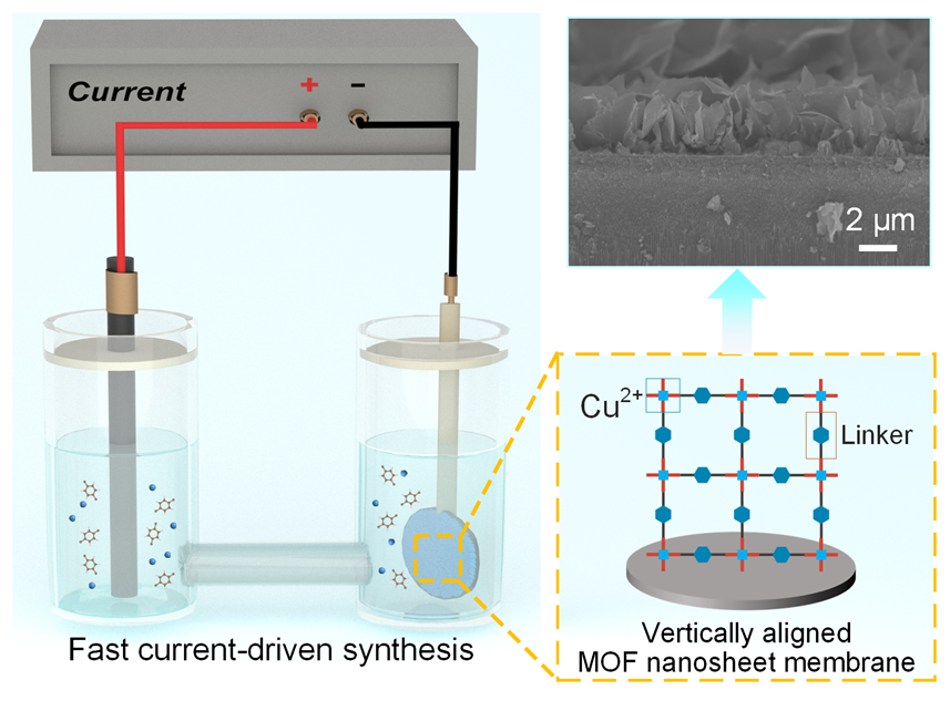
本研究通过一种快速电流驱动策略, 在短短10 min内原位构筑出具有垂直结构的MOF纳米片膜(图1). 该策略利用电化学作用促进配体脱质子, 加快MOF纳米片在基底的快速成核与生长. 随着反应进行, 晶体水平生长受阻, 生长方向由原先的平行取向逐渐转为垂直排列. 相较于传统水平堆叠膜结构, 该垂直排列结构显著改善了气体分子的扩散路径, 避免了因水平堆叠而造成的传质瓶颈. 气体分离测试结果表明, 所制备的垂直排列的MOF纳米片膜对H2具有极高的渗透性能, 其渗透率达到1.5×10⁻⁶ mol•m-2•s-1•Pa-1, 较传统的水平堆叠MOF纳米片膜提升了5倍. 同时, 该膜在H2/CO2体系中表现出不错的选择性(20).
2 结果与讨论
2.1 MOF纳米片膜的制备
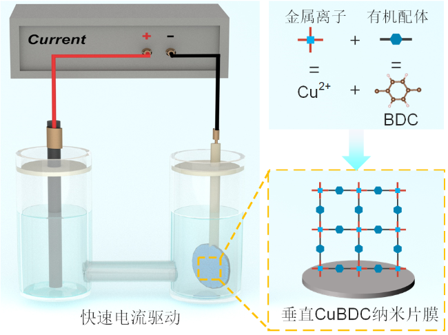
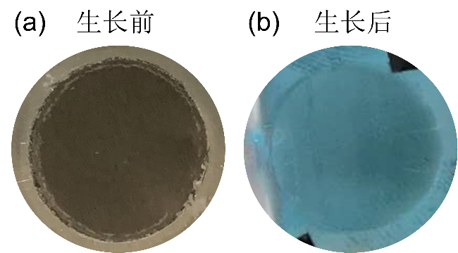
本研究以二维层状MOF材料CuBDC (Copper 1,4-benzenedicarboxylate)为研究对象. 该材料由铜离子(Cu2+)与1,4-苯二甲酸(BDC)有机配体通过配位键自组装形成具有周期性网状结构的配位聚合物, 因其出色的结构可调控性和丰富规整的纳米通道, 是目前MOF纳米片研究中最具代表性的材料之一, 兼具代表性与应用潜力[17-20]. 为突破传统组装方式的局限, 本研究采用了一种快速电流驱动策略, 在导电基底上实现CuBDC膜的原位快速构建. 基于阴极沉积的电流驱动策略, 通过电化学作用促进BDC配体脱质子[21-22], 从而加快CuBDC纳米片在基底上的原位成核与生长. 同时, Cu2+阳离子在电场作用下被吸引至电极附近, 进一步推动了膜的快速组装. 在MOF膜的合成过程中, 基底上的异相成核有利于形成连续的膜层, 而溶液中出现的均相结晶则降低膜的完整性[23]. 为了提高MOF膜的异相成核效率, 本研究预先在基底表面喷涂铂(Pt)层, 通过增加成核位点密度有效促进了CuBDC的异相成核与生长(图2a). 随后将预先涂覆Pt层的多孔阳极氧化铝(AAO)基底浸没于CuBDC前体溶液中, 于–0.7 mA/cm2的小电流密度下沉积一段时间后, 基底颜色由深棕色转变成蓝色, 表明CuBDC纳米片已成功生长到基底表面(图2b).
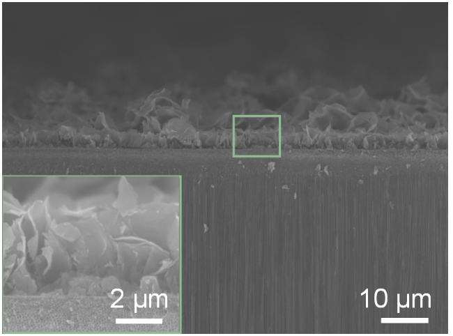
通过控制反应时间, 实现了CuBDC纳米片膜在AAO基底上的可控生长. 图3(b~f)展示了膜在不同反应时间下的形貌演变过程. 在反应初期(施加电流约1 min后), 电化学作用促使金属离子与有机配体快速形成纳米级前驱体, 并均匀分布在AAO基底表面(图3a和3b). 该前驱层类似于“种子”层, 有效降低了成核能垒, 为MOF生长提供了密集的异质成核位点. 此阶段AAO基底孔结构仍清晰可见, 说明成核尚未完全覆盖. 随着反应进行(约2~4 min), CuBDC晶体开始选择性地在前驱体诱导下生长, 初步形成CuBDC纳米片结构(图3c). 4 min时, 纳米片逐渐连接扩展, 在平面方向初步形成连续膜并出现垂直取向. 这是因为随着膜层进一步增长, 原始水平生长方向所受的空间阻力不断加剧, 根据Van der Drift竞争性生长理论[24-25], 晶体生长方向将倾向于“低阻力路径”演化, 即逐步由平行生长转变为垂直取向. 但此阶段膜层仍未完全覆盖, 部分区域存在裸露孔道(图3d). 反应延长至10 min后, CuBDC纳米片垂直排列并构筑出完整且连续的膜层(图3e), 膜厚约为4.5 μm(图4). 此时膜的绝缘特性导致系统电流信号明显下降, 表明基底表面已被MOF膜完全覆盖, 电荷传导受限, 这一电化学信号可作为膜完整性的有效指标[12]. 反应持续至20 min后(图3f), CuBDC纳米片沿垂直方向进一步堆叠, 形成明显的多层结构, 验证了晶体在垂直方向优先生长的趋势.
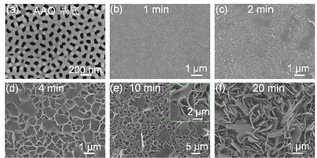
图3 (a)涂覆Pt层的AAO基底与(b~f)基于不同反应时间制备的CuBDC纳米片膜的表面SEM图像Figure 3 Top-view SEM images of (a) AAO substrate coated with Pt layer and (b~f) CuBDC nanosheet membranes prepared at different reaction times |
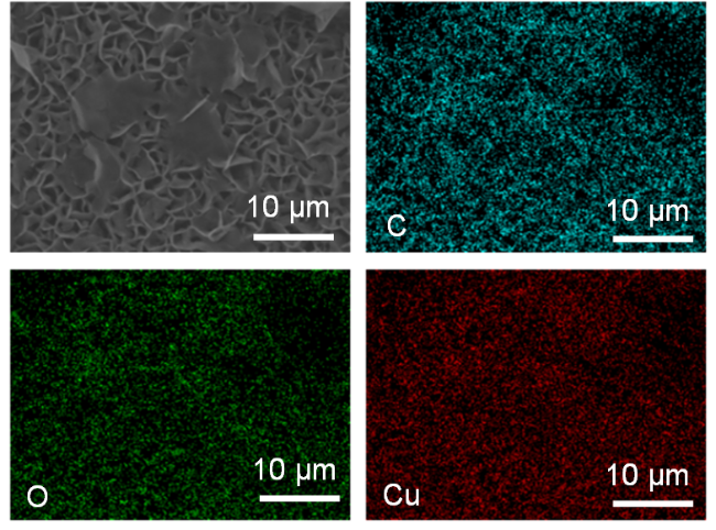
X射线衍射(XRD)结果与扫描电子显微镜(SEM)所观察到的结果高度一致, 揭示了CuBDC纳米片膜从“非晶到高结晶”的演变过程. 如图5a所示, 反应初期(1 min)未检测到明显衍射峰, 表明晶体尚未形成, 仍处于成核前期. 随着反应时间延长, [001]晶面的衍射峰显现并逐渐增强, 证实CuBDC晶体开始形成且结晶程度持续提高. 反应10 min后, XRD图谱显示[001]晶面衍射峰占主导, 表明纳米片膜呈现高度[001]择优取向特性. 结合晶体结构分析可知(图5b和5c), 膜表面暴露出规则有序的孔道结构(理论孔径: 0.52 nm)[18,26], 为气体分子提供了高效传输通道. 能谱分析(EDS)进一步证实C、O、Cu元素在膜中均匀分布, 表明CuBDC纳米片膜已在基底上实现均匀生长(图6).
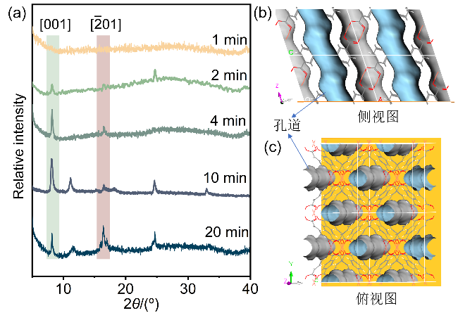
图5 (a)基于不同反应时间制备的CuBDC纳米片膜的XRD图谱; CuBDC晶体沿[001]方向的(b)侧视图与(c)俯视图Figure 5 (a) XRD patterns of the CuBDC nanosheet membranes prepared at different reaction times. (b) Side and (c) top views of CuBDC crystal along the [001] direction |
2.2 分离性能测试
CuBDC纳米片膜的气体分离性能与其结构演变密切相关. 随着反应时间的增加, 膜结构经历了从稀疏成核、水平连接到垂直排列再到过度堆叠的逐步演化, 这一演化直接影响了膜结构和气体传输路径, 最终决定了膜的分离性能.
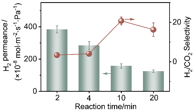
如图8所示, CuBDC纳米片膜的H2渗透率随生长时间延长而持续下降, 而H2/CO2选择性呈现先升后降的趋势. 反应初期(4 min)的膜表现出高H2渗透率(3.4×10⁻⁶ mol•m-2•s-1•Pa-1)但选择性低(≈3.3), 这是由于不连续的膜层存在非选择性传输通道, 而非MOF自身孔道. 这可以从不同反应时间制备的CuBDC纳米片膜表面SEM图中得以证实(图3). 当反应时间增至10 min, 膜结构趋于致密且纳米片垂直排列, 气体主要通过MOF孔道进行有序传输, 此时CuBDC膜的H2/CO2选择性达到最高值(约20), 同时H2渗透率仍保持在较高水平(1.5×10⁻⁶ mol•m-2•s-1•Pa-1). 该垂直结构显著缩短了气体分子的扩散路径, 降低了传质阻力. 当反应时间延长至20 min时, CuBDC纳米片膜的H2渗透率和H2/CO2选择性均出现小幅下降. 虽然膜的垂直取向结构得以保持, 但MOF纳米片的过度堆叠会阻碍H2扩散, 导致渗透率降低. 由此可见, 10 min制备的垂直排列膜在结构完整性和传质效率间达到最佳平衡, 展现出最优的气体渗透-选择性协同效应, 最终被确定为后续单气体测试的最佳制膜参数.
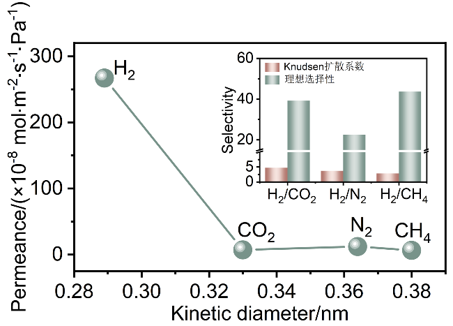
随后, 探究了反应10 min制备的CuBDC纳米片膜的单气体渗透性能. 如图9所示, CuBDC纳米片膜展现出最高的H2渗透率, 高达2.7×10⁻⁶ mol•m-2•s-1•Pa-1, 远高于其他气体的渗透率. 相应的H2/CO2、H2/N2和H2/CH4理想选择性分别为39.2、22.4和43.6, 远超Knudsen扩散系数. 尽管CuBDC的理论孔径(0.52 nm)大于所有测试气体分子的动力学直径, 但其仍展现出较高的H2/CO2和H2/CH4选择性, 表明分离机制由吸附与扩散协同作用驱动. 首先, 较大分子在膜内扩散阻力较高[30], 而H2分子则能够更快地通过膜. 其次, CuBDC金属位点与CO2之间存在强大的相互作用[31], 导致CO2分子在膜内传输困难. 而CH4分子则与框架芳香环形成C—H…π静电相互作用, 增强了其在膜内的吸附, 从而影响了CH4在膜内的传输[32]. 同时, 部分被吸附的CO2或CH4分子会占据部分孔道, 导致孔径减小, 增加了CO2或CH4的传输阻力, 从而提高了气体选择性. 最终, 这两个因素共同导致了相对较高的H2/CO2和H2/CH4选择性. 此外, 从实验结果来看, 混合气体分离中H2分子的渗透率(PH2: 1.5×10⁻⁶ mol•m-2•s-1•Pa-1)明显低于其在单气体测试中的渗透率(PH2: 2.7×10⁻⁶ mol•m-2•s-1• Pa-1), 这表明, 吸附在膜上的CO2分子也会影响混合气体中H2的扩散.
为进一步验证垂直取向结构在气体分离中的优势, 我们设计了对比实验, 采用传统水平堆叠方式制备了水平排列的CuBDC纳米片膜(简称“水平膜”). 采用自下而上的策略合成了CuBDC纳米片, 其平均横向尺寸约为1.5 μm(图10a), 并通过抽滤方式使其在AAO基底上形成水平堆叠的膜结构(图10b). XRD结果显示(图11a), CuBDC纳米片及其相应的水平堆叠膜均表现出显著的$[\bar{2}01] $晶面择优取向, 表明膜表面暴露出一维有序孔道(理论孔径为0.52 nm)[26](图11b). 同时, 该实验衍射结果与CuBDC的模拟衍射结果高度吻合, 充分证明了纳米片的成功制备. SEM截面显示膜厚为4 μm(图10b), 与基于快速电流驱动策略制备的垂直取向CuBDC纳米片膜(简称“垂直膜”)厚度相当.
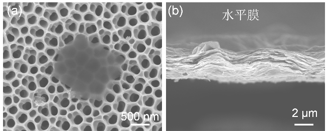
图10 (a) CuBDC纳米片的SEM图像; (b)水平堆叠CuBDC纳米片膜的横截面SEM图像Figure 10 (a) SEM image of CuBDC nanosheet; (b) SEM cross-sectional view of horizontally stacked CuBDC nanosheet membrane |
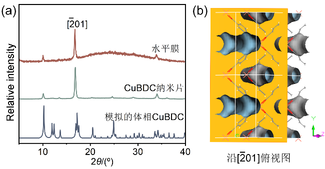
图11 (a)模拟的体相CuBDC、传统方法制备的CuBDC纳米片及相应的水平堆叠膜的XRD图谱对比; (b) CuBDC晶体沿$[\bar{2}01] $方向的俯视图Figure 11 (a) Comparison of XRD patterns of simulated bulk CuBDC, CuBDC nanosheets synthesized via the conventional method, and the corresponding horizontally stacked membrane; (b) top view of CuBDC crystal along the $[\bar{2}01] $ direction |
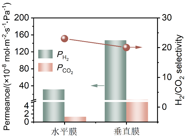
随后对比了两种不同排列结构的CuBDC纳米片膜的气体分离性能, 评估其在相同厚度条件下的分离能力. 为确保对比的合理性与结论的可靠性, 所有气体分离实验均在完全一致的测试条件(测试温度: 25 ℃、进料压力: 0.1 MPa)下进行. 如图12所示, 垂直膜展现出优于水平膜的H2渗透性能, 其渗透率高达1.5×10⁻⁶ mol•m-2•s-1•Pa-1, 较水平膜提升了5倍, 且两者在H2/CO2选择性方面差异相对较小, 这说明了垂直排列结构通过缩短气体传质路径, 可显著提升气体分子传输效率.
3 结论
本研究采用快速电流驱动原位生长策略, 在10 min内成功构建了垂直排列的CuBDC纳米片膜. 该结构显著缩短了气体分子扩散路径, 克服了水平堆叠带来的传质瓶颈问题, 使CuBDC纳米片膜的H2渗透率高达 1.5×10⁻⁶ mol•m-2•s-1•Pa-1, 较水平堆叠膜提高5倍, 同时保持H2/CO2分离选择性约20. 该研究不仅证实了垂直取向结构在提升分子传质效率方面的关键作用, 也为MOF纳米片膜的快速构筑与传质路径优化提供了新的设计思路与理论支持.
4 实验部分
前体溶液的制备: 将0.03 g三水合硝酸铜(Cu(NO3)2•3H2O)溶于1 mL N,N-二甲基甲酰胺(DMF)和3 mL乙腈(MeCN)的混合溶液中形成A液; 将0.03 g BDC溶于3 mL DMF和1 mL MeCN的混合溶液中形成B液[18]. 所得A或B溶液经超声处理以确保所有组分完全溶解, 随后将A加入到B中充分混合最终得到用于CuBDC膜合成的均相前体溶液.
快速电流驱动法制备垂直CuBDC纳米片膜: 将预先涂覆Pt层的AAO基底浸没于上述制备好的CuBDC前体溶液中, 于室温下施加电流密度为–0.7 mA/cm2进行电化学沉积一段时间, 随后取出并于室温下自然干燥, 即可获得垂直CuBDC纳米片膜.
CuBDC纳米片和水平堆叠结构的纳米片膜的制备: 将上述CuBDC前体溶液在室温条件下静置反应12 h, 以促进纳米片的自组装形成. 反应结束后, 使用高速离心(10000 r/min, 30 min)收集产物, 使用DMF洗涤3次, 接着再用二氯甲烷(CH2Cl2)洗涤3次, 以去除残留未反应配体. 洗涤后的纳米片分散在CH2Cl2中, 制得稳定的纳米片悬浮液, 并置于密闭容器中于室温储存, 备用.
将制备好的CuBDC纳米片悬浮液取一定体积, 通过抽滤方式将纳米片均匀沉积在AAO基底表面. 沉积完成后, 放置在室温条件下自然干燥24 h, 最终获得具有水平堆叠结构的CuBDC纳米片膜.
(Cheng, B.)