


1 引言
2 结果与讨论
2.1 活性层材料的光电特性
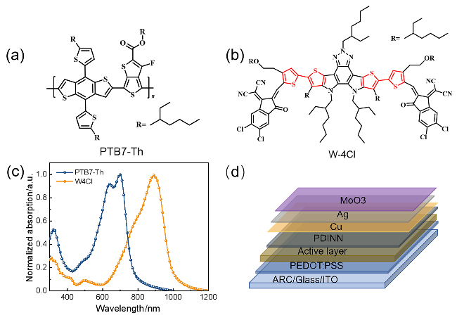
图1 (a)聚合物给体材料PTB7-Th; (b)近红外小分子受体材料W-4Cl的分子结构式; (c) PTB7-Th和W-4Cl薄膜的紫外-可见吸收光谱; (d)半透明有机太阳能电池的结构示意图Figure 1 (a) Polymer donor material PTB7-Th; (b) Molecular structure of NIR small molecule acceptor material W-4Cl; (c) UV-visible absorption spectra of PTB7-Th and W-4Cl thin films; (d) Device structure of semi-transparent organic solar cell |
表1 PTB7-Th和W-4Cl薄膜的吸收特性Table 1 Absorption properties of PTB7-Th and W-4Cl films |
| Donor/Acceptor | λmax/nm | λonset/nm | Eopt/eV |
|---|---|---|---|
| PTB7-Th | 698 | 770 | 1.61 |
| W-4Cl | 892 | 990 | 1.25 |
2.2 不透明器件光伏性能
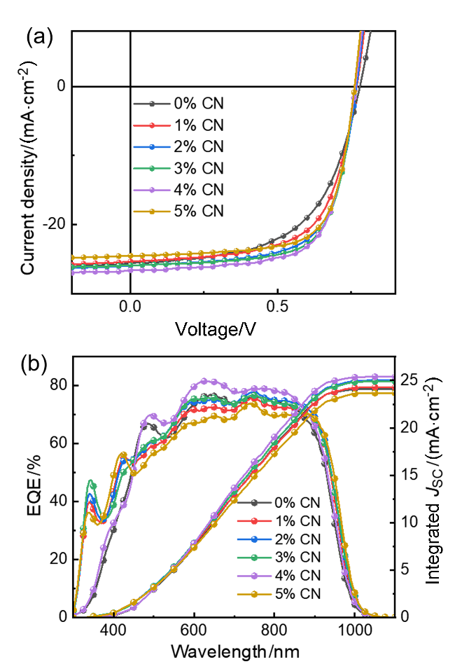
图2 不同添加剂含量的PTB7-Th:W-4Cl基不透明器件的(a) J-V曲线和(b) EQE曲线Figure 2 (a) J-V curve and (b) EQE curve of PTB7-Th:W-4Cl-based opaque device with different additive content |
表2 不同添加剂含量的PTB7-Th:W-4Cl基不透明器件光伏参数Table 2 Photovoltaic parameters of the PTB7-Th:W-4Cl-based opaque device with different additive content |
| φ(CN)/% | VOC/V | JSC/(mA•cm−2) | FF/% | Jcal/(mA•cm−2) | PCE/% |
|---|---|---|---|---|---|
| 0 | 0.780 | 25.31 | 57.65 | 24.11 | 11.23 |
| 1 | 0.769 | 25.33 | 64.11 | 24.29 | 12.50 |
| 2 | 0.768 | 25.93 | 66.81 | 25.01 | 13.32 |
| 3 | 0.764 | 25.87 | 69.33 | 24.90 | 13.73 |
| 4 | 0.764 | 26.59 | 68.44 | 25.39 | 14.10 |
| 5 | 0.762 | 24.50 | 70.33 | 23.68 | 13.15 |
表3 已报道的PTB7-Th基OSCs性能参数Table 3 Photovoltaic parameters of the previously reported OSCs based on PTB7-Th |
| Blend film | VOC/V | JSC/(mA•cm−2) | FF/% | PCE/% | Ref. |
|---|---|---|---|---|---|
| PTB7-Th:PC71BM | 0.79 | 16.92 | 71.5 | 9.54 | [24] |
| PTB7-Th:MDCzM-4H | 1.03 | 15.87 | 62.2 | 10.17 | [25] |
| PTB7-Th:MDCzM-4F | 0.965 | 20.92 | 69.8 | 14.09 | [25] |
| PTB7-Th:L8-BO | 0.72 | 23.4 | 62.4 | 10.5 | [26] |
| PTB7-Th:BTPSV-4F | 0.66 | 28.4 | 69.5 | 13.0 | [27] |
| PTB7-Th:BTPSeV-4F | 0.66 | 30.1 | 71.4 | 14.2 | [27] |
| PTB7-Th: BZO-4Cl | 0.706 | 28.33 | 70.62 | 14.12 | [11] |
| PTB7-Th:COTIC-4F | 0.551 | 24.95 | 61 | 8.41 | [28] |
| PTB7-Th:ATT-9 | 0.663 | 30.0 | 67.2 | 13.35 | [29] |
| PTB7-Th:DTC-T-F | 0.78 | 17.46 | 65 | 8.8 | [30] |
| PTB7-Th:F-BTA5 | 1.03 | 15.29 | 65.78 | 10.36 | [31] |
| PTB7-Th:3TT-FIC | 0.66 | 25.89 | 71.20 | 12.21 | [32] |
| PTB7-Th:O-IDTBR | 1.00 | 15.2 | 63.0 | 9.57 | [33] |
| PTB7-Th: FOIC | 0.734 | 22.94 | 65.33 | 11.01 | [34] |
2.3 激子解离、电荷传输和电荷复合
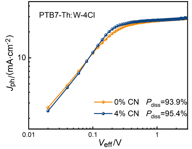
表4 含0%和4% CN的PTB7-Th:W-4Cl器件的电荷传输性能参数Table 4 Detailed charge transport performance for PTB7-Th:W-4Cl devices with 0% and 4% CN |
| Blend film | Pdiss | Pcoll | α | nkT/q | μh/(cm2•V−1•s−1) | μe/(cm2•V−1•s−1) | μe/μh |
|---|---|---|---|---|---|---|---|
| 0% CN | 93.9% | 73.8% | 0.995 | 1.20 | 6.6×10⁻⁵ | 5.3×10⁻⁵ | 0.803 |
| 4% CN | 95.4% | 81.4% | 0.999 | 1.19 | 7.6×10⁻⁵ | 8.2×10⁻⁵ | 1.079 |
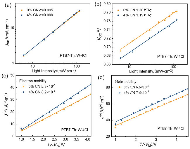
图4 基于0% CN和4% CN的PTB7-Th:W-4Cl器件: (a) JSC-Plight特性曲线; (b) VOC-Plight特征曲线; (c)电子迁移率曲线; (d)空穴迁移率曲线Figure 4 PTB7-Th:W-4Cl device with 0% CN and 4% CN content: (a) Characteristic curve of JSC-Plight; (b) Characteristic curve of VOC-Plight; (c) Electron mobility curve; (d) Hole mobility curve |
2.4 高效半透明器件
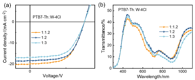
图5 (a)不同D/A比值PTB7-Th:W-4Cl半透明器件的J-V曲线; (b)透射曲线Figure 5 (a) J-V curves of PTB7-Th:W-4Cl semi-transparent devices with different D/A ratios; (b) Transmittance curve |
表5 不同D/A比的PTB7-Th:W-4Cl半透明器件性能Table 5 Photovoltaic performance of PTB7-Th:W-4Cl semi-transparent devices with different D/A ratios |
| D/A Ratio | VOC/V | JSC/(mA•cm−2) | FF/% | PCE/% | CRI | AVT/% | LUE/% |
|---|---|---|---|---|---|---|---|
| 1∶1.2 | 0.757 | 19.92 | 57.4 | 8.67 | 69.84 | 30.44 | 2.63 |
| 1∶2 | 0.756 | 18.33 | 60.3 | 8.38 | 75.55 | 33.51 | 2.81 |
| 1∶3 | 0.755 | 16.76 | 57.7 | 7.32 | 76.21 | 33.90 | 2.48 |
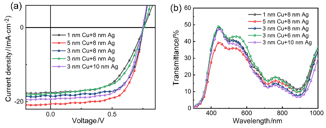
图6 (a)不同顶部电极结构的PTB7-Th:W-4Cl半透明器件J-V曲线; (b)透光率曲线Figure 6 (a) J-V curves of PTB7-Th:W-4Cl semi-transparent devices with different top electrode structures; (b) Transmittance curve |
表6 不同顶部电极结构PTB7-Th:W-4Cl半透明器件的性能参数Table 6 Photovoltaic performance parameters of PTB7-Th:W-4Cl semi-transparent devices with different top electrode structures |
| Top electrode structures | VOC/V | JSC/(mA•cm−2) | FF/% | PCE/% | AVT/% | LUE/% |
|---|---|---|---|---|---|---|
| 3 nm Cu+6 nm Ag | 0.757 | 17.78 | 58.1 | 7.82 | 38.92 | 3.04 |
| 3 nm Cu+8 nm Ag | 0.754 | 18.45 | 65.4 | 9.11 | 36.05 | 3.28 |
| 3 nm Cu+10 nm Ag | 0.747 | 19.29 | 64.5 | 9.31 | 31.73 | 2.95 |
| 1 nm Cu+8 nm Ag | 0.757 | 17.49 | 56.6 | 7.43 | 36.99 | 2.74 |
| 5 nm Cu+8 nm Ag | 0.753 | 20.59 | 66.3 | 10.19 | 27.56 | 2.80 |
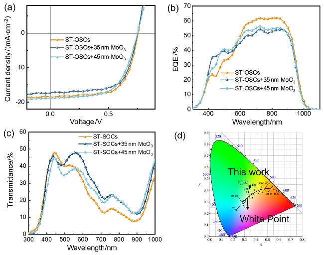
图7 (a)不同MoO3结构的PTB7-Th:W-4Cl半透明器件J-V曲线; (b) EQE曲线; (c)透射率曲线; (d) CIE 1931xyz色度图Figure 7 (a) J-V curves of PTB7-Th:W-4Cl semi-transparent devices with different MoO3 structures; (b) EQE curve; (c) Transmittance curve; (d) CIE 1931xyz chromaticity diagram |
表7 不同MoO3结构的半透明器件性能参数Table 7 Photovoltaic performance parameters of semi-transparent devices with different MoO3 structures |
| Top electrode structures | VOC/V | JSC/(mA•cm−2) | FF/% | PCE/% | CRI | AVT/% | LUE/% |
|---|---|---|---|---|---|---|---|
| 3 nm Cu+8 nm Ag | 0.754 | 18.45 | 65.4 | 9.11 | 75.52 | 36.05 | 3.28 |
| +35 nm MoO3 | 0.750 | 17.30 | 66.1 | 8.58 | 86.53 | 44.45 | 3.81 |
| +45 nm MoO3 | 0.750 | 17.73 | 61.0 | 8.12 | 87.11 | 36.27 | 2.95 |
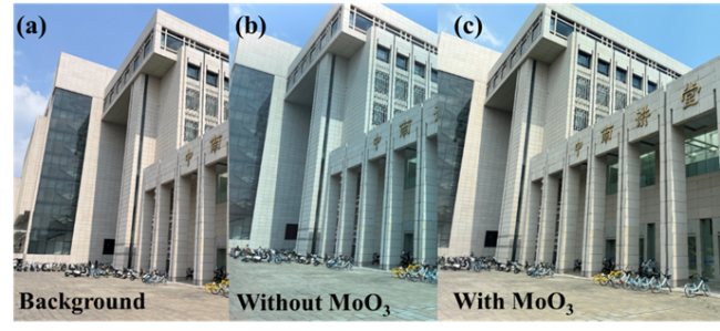
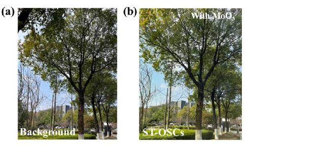
图8 (a)背景图; (b)未沉积MoO3和(c)沉积35 nm MoO3 PTB7-Th: W-4Cl半透明器件(附在相机上), 以中南讲堂为背景拍摄Figure 8 (a) Background picture; (b) Unvaporized MoO3 and (c) Vaporized 35 nm MoO3 PTB7-Th:W-4Cl semi-transparent device attached to the camera, taken with the Central South Lecture Hall |