化学学报 ›› 2022, Vol. 80 ›› Issue (12): 1643-1663.DOI: 10.6023/A22080347 上一篇 下一篇
综述
叶淳懿, 邬学贤, 张志彬, 丁萍, 骆静利, 符显珠*( )
)
投稿日期:2022-08-06
发布日期:2022-09-16
通讯作者:
符显珠
作者简介: |
叶淳懿, 深圳大学材料学院材料与化工专业在读硕士研究生, 研究方向为面向电子与能源领域应用的化学镀技术及其活化剂. |
 |
符显珠, 深圳大学材料学院教授, 博士生导师, 从事电化学能源材料与器件及电子材料与制程研究. 2007年厦门大学化学系博士毕业, 2008~2012年在加拿大阿尔伯塔大学做博士后并到美国伯克利国家实验室进行访问研究, 曾于中国科学院深圳先进技术研究院工作. 近5年以通讯作者在Nature Catalysis、Journal of the American Chemical Society、Angewandte Chemie、Energy & Environmental Science、Science Bulletin(科学通报)等期刊发表SCI论文100多篇. |
基金资助:
Chunyi Ye, Xuexian Wu, Zhibin Zhang, Ping Ding, Jing-Li Luo, Xian-Zhu Fu()
Received:2022-08-06
Published:2022-09-16
Contact:
Xian-Zhu Fu
Supported by:文章分享

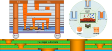
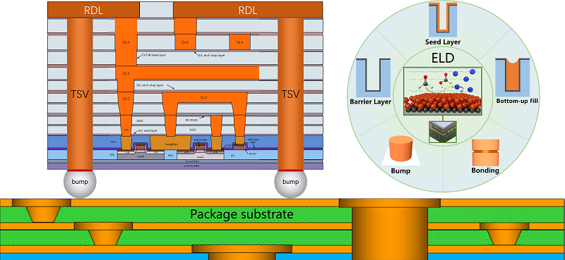
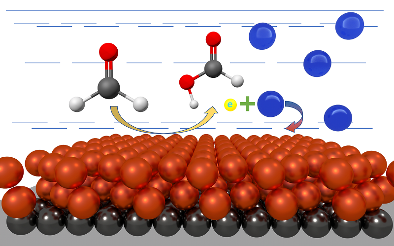
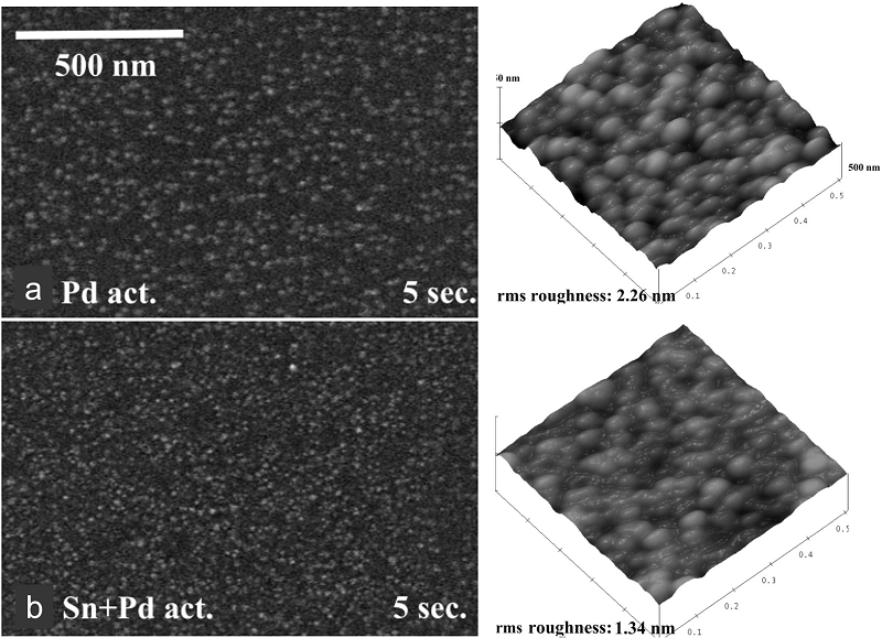
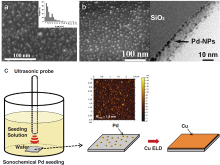
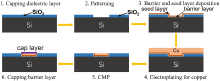
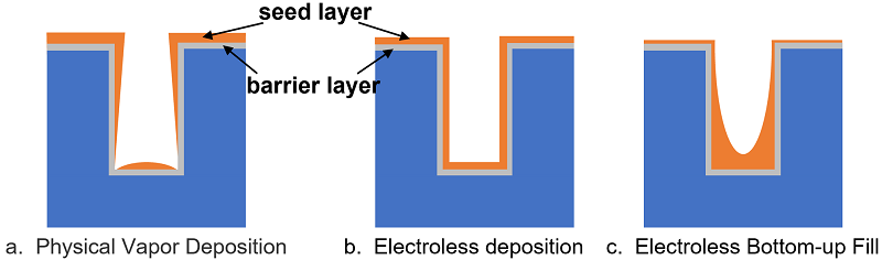
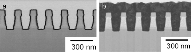
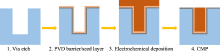
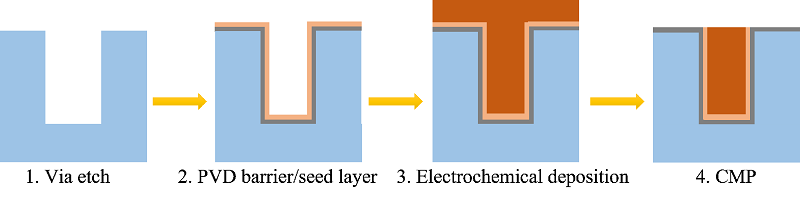
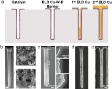
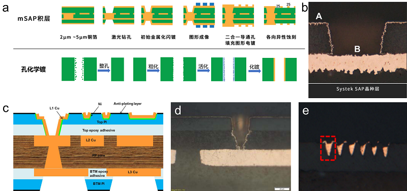
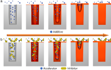
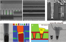
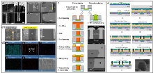
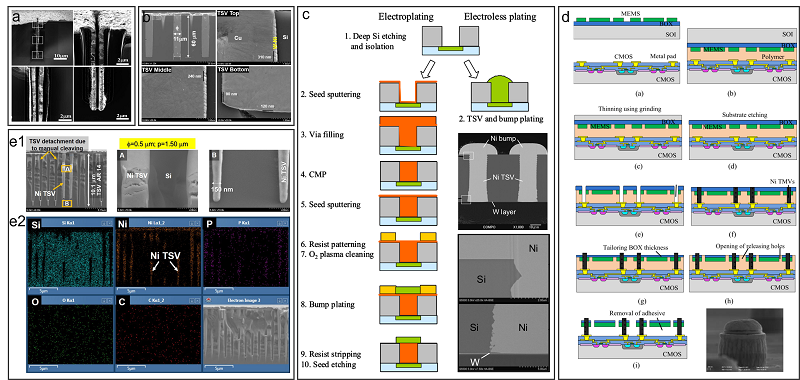
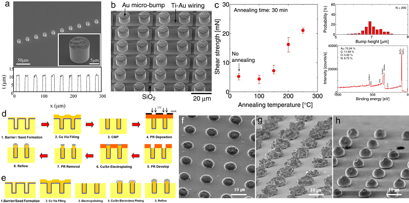
芯片制造中大量使用物理气相沉积、化学气相沉积、电镀、热压键合等技术来实现芯片导电互连. 与这些技术相比, 化学镀因具有均镀保形能力强、工艺条件温和、设备成本低、操作简单等优点, 被人们期望应用于芯片制造中, 从而在近年来得到大量的研究. 本综述首先简介了芯片制造中导电互连包括芯片内互连、芯片3D封装硅通孔(TSV)、重布线层、凸点、键合、封装载板孔金属化等制程中传统制造技术与化学镀技术的对比, 说明了化学镀用于芯片制造中的优势; 然后总结了芯片化学镀的原理与种类、接枝与活化前处理方法和关键材料; 并详细介绍了芯片内互连和TSV互连化学镀阻挡层、种子层、互连孔填充、化学镀凸点、再布线层、封装载板孔互连种子层以及凸点间键合的研究进展; 且讨论了化学镀液组成及作用, 超级化学镀填孔添加剂及机理等. 最后对化学镀技术未来应用于新一代芯片制造中进行了展望.
叶淳懿, 邬学贤, 张志彬, 丁萍, 骆静利, 符显珠. 芯片制造中的化学镀技术研究进展[J]. 化学学报, 2022, 80(12): 1643-1663.
Chunyi Ye, Xuexian Wu, Zhibin Zhang, Ping Ding, Jing-Li Luo, Xian-Zhu Fu. Research Progress of Electroless Plating Technology in Chip Manufacturing[J]. Acta Chimica Sinica, 2022, 80(12): 1643-1663.

| ELD metal | Reaction | Application in chip manufacturing |
|---|---|---|
| Cu | Cu2++2HCHO+4OH‒→ Cu0+2HCOO‒+2H2O+H2 | Seed layer, gap filling, bump |
| Ni | Ni2++2H2O+2H2PO2‒→Ni0+4H++2HPO32‒+H2 | Barrier layer, activator layer, UBM |
| Au | Au(SO3)23‒+e‒+H2O→SO32‒+SO2+Au+2OH‒ | Bump, UBM |
| Co | Co2++2H2O+2H2PO2‒→Co0+4H++2HPO32‒+H2 | Barrier layer, gap filling |
| Pd | Pd2++2H2O+2H2PO2‒→Pd0+4H++2HPO32‒+H2 | UBM |

| Molecular name | Abbreviations | Head group | References |
|---|---|---|---|
| 3-Aminopropyltriethoxysilane | APTES/Am1 | —NH2 | [ |
| Aminopropyltrimethoxysilane | APTMS/APS | —NH2 | [ |
| n-(2-Aminoethyl)-3-aminopropyl-trimethoxysilane | AEAPTMS/Am2 | —NH2 | [ |
| 2-(Trimethoxysilyl)-ethylpyridine | Py | —C5H4N | [ |
| N-(3-Trimethoxysilylpropyl) diethylenetriamine | TPDA | —NH2 | [ |
| Alkyl(octadecyltrichlorosilane) | OTS | —CH3 | [ |
| 3-[2-(2-Aminoethylamino)ethylamino]-propyltrimethoxysilane | ETAS | —NH2 | [ |
| (3-Mercaptopropyl)trimethoxysilane | MPTMS | —SH | [ |


| Activator | Process | References |
|---|---|---|
| PdCl2 | Absorb, reduce | [ |
| Ni(NO3)2 | Absorb, reduce | [ |
| Pd | Absorb | [ |
| Au | Absorb | [ |
| Pd Layer | ICB | [ |
| K2PdCl6 | Sonochemical reduce | [ |
| Cu Film | Sputter | [ |
| Ru Layer | ALD | [ |
| NiB Layer | ELD | [ |
| Activator | Process | References |
|---|---|---|
| PdCl2 | Absorb, reduce | [ |
| Ni(NO3)2 | Absorb, reduce | [ |
| Pd | Absorb | [ |
| Au | Absorb | [ |
| Pd Layer | ICB | [ |
| K2PdCl6 | Sonochemical reduce | [ |
| Cu Film | Sputter | [ |
| Ru Layer | ALD | [ |
| NiB Layer | ELD | [ |


| Source of metal | Reducing agent | Additives | pH | Temperature/℃ | References |
|---|---|---|---|---|---|
| NiSO4•6H2O (NH4)2ReO4 | NaH2PO2•H2O | Sodium citrate | 9.0 (adjusted with NaOH) | 90 | [ |
| NiSO4 | DMAB | Citric acid monohydrate | 9.0 (adjusted with TMAH) | 70 | [ |
| NiSO4•7H2O Na2MoO4•6H2O | NaH2PO2 | C6H5Na3O7•H2O SDS | 9~10 | 85~90 | [ |
| Nickel chloride | Sodium hypophosphite Sodium borohydride | Ammonium citrate dibasic Ethylenediamine Sodium dodecyl sulfate Saccharine | 13 (adjusted with NaOH) | 65 | [ |
| Nickel sulfate | DMAB | Citric acid SPS | 9.5 | 70 | [ |
| NiSO4•6H2O | DMAB | C6H5Na3O7•2H2O | 9 | 65 | [ |
| NiSO4•6H2O | NaH2PO2•H2O | C6H5Na3O7•3H2O | 5.5 (adjusted with NH3•H2O) | 80 | [ |
| NiSO4•6H2O Na2WO4•2H2O | NaH2PO2•H2O | Na3C6H8O7•2H2O | 7.0~9.0 | 80~95 | [ |

| Source of metal | Reducing agent | Additives | pH | Temperature/℃ | References |
|---|---|---|---|---|---|
| CoSO4•6H2O Na2MoO4•2H2O | NaH2PO2 | Na-citrate RE610 H3BO3 | 8.9~9.0 (adjusted with KOH) | — | [ |
| CoSO4•7H2O Na2WO4•2H2O | NaH2PO2•H2O | Na3C6H5O7•2H2O H3BO3 | 9 (adjusted with KOH) | 85 | [ |
| CoSO4•7H2O Na2WO4 | DMAB NaH2PO2 | Na3C6H5O7•2H2O RE610 HCl | 9.5~9.7 (adjusted with NaOH) | 20~85 | [ |
| CoCl2•6H2O Na2WO4•2H2O | DMAB | H3C6H5O7•H2O | 9.5 (adjusted with TMAH) | 75 | [ |
| CoSO4•7H2O Na2WO4•2H2O | NaH2PO2 | 3Na-citrate H3BO3 | 8~12 | 90 | [ |
| Cobalt sulfate Tungsten acid | DMAB | Citric acid | 9.5 (adjusted with TMAH) | 70 | [ |
| Cobalt sulfate Tungsten acid | DMAB | Citric acid SPS | 9.5 | 60 | [ |
| Cobalt sulfate | DMAB | Citric acid | 9.5 | 70 | [ |

| Source of metal | Reducing agent | Additives | pH | Temperature/℃ | References |
|---|---|---|---|---|---|
| CuSO4•5H2O | Paraformaldehyde | EDTA | — (adjusted with KOH) | 70 | [ |
| CuSO4•5H2O | Glyoxylic acid | EDTA Surfactant RE-610 | 12.3~12.7 (adjusted with KOH) | 65~75 | [ |
| CuSO4•5H2O | HCHO | KNaC4H4O6•4H2O 2,2'-dipyridyl Na2S2O3•5H2O NiCl2•6H2O | 12~14 (adjusted with NaOH and Na2CO3) | 25 | [ |
| CuSO4•5H2O | Glyoxylic acid | EDTA 2,2'-dipyridine PEG | 12.7 (adjusted with TMAH) | 60 or 70 | [ |
| CuSO4•5H2O | HCHO | EDTA PEG | 12.6~12.7 (adjusted with NaOH) | 45 | [ |
| CuSO4•5H2O MnSO4•H2O | HCHO | C4H4KNaO6•4H2O | 13 (adjusted with NaOH) | — | [ |
| CuSO4•5H2O | Glyoxylic acid | EDTA PEG-Thiol | 12.5 | 70 | [ |


| [18] |
Gebrael, T.; Li, J.; Gamboa, A. R.; Ma, J.; Schaadt, J.; Horowitz, L.; Pilawa-Podgurski, R.; Miljkovic, N. Nat. Electron. 2022, 5, 394.
|
| [19] |
Wang, Q.; Sun, Y.-X.; Zhang, B. Printed Circ. Inform. 2022, 30, 24. (in Chinese)
|
|
( 王群, 孙宇曦, 张波, 印制电路信息, 2022, 30, 24.)
|
|
| [20] |
Ghosh, S. Thin Solid Films 2019, 669, 641.
|
| [21] |
Zheng, A.-N.; Jin, L.; Yang, J.-Q.; Li, W.-Q.; Wang, Z.-Y.; Yang, F.-Z.; Zhan, D.-P.; Tian, Z.-Q. Acta Chim. Sinica 2022, 80, 659. (in Chinese)
doi: 10.6023/A22010026 |
|
( 郑安妮, 金磊, 杨家强, 李威青, 王赵云, 杨防祖, 詹东平, 田中群, 化学学报 2022, 80, 659.)
doi: 10.6023/A22010026 |
|
| [22] |
Chen, S.-T.; Chung, Y.-C.; Fang, J.-S.; Cheng, Y.-L.; Chen, G.-S. Appl. Surf. Sci. 2017, 405, 350.
|
| [23] |
Bernasconi, R.; Molazemhosseini, A.; Cervati, M.; Armini, S.; Magagnin, L. J. Electron. Mater. 2016, 45, 5449.
|
| [24] |
Malki, M.; Rozenblat-Raz, A.; Duhin, A.; Inberg, A.; Horvitz, D.; Shacham-Diamand, Y. Surf. Coat. Technol. 2014, 252, 1.
|
| [25] |
Wu, P.-H.; Lai, Y.-Z.; Zhang, Y.-P.; Sil, M. C.; Lee, P.-H. H.; Wei, T.-C.; Chen, C.-M. ACS Appl. Nano Mater. 2020, 3, 3741.
|
| [26] |
Inoue, F.; Shimizu, T.; Miyake, H.; Arima, R.; Ito, T.; Seki, H.; Shinozaki, Y.; Yamamoto, T.; Shingubara, S. Electrochim. Acta 2012, 82, 372.
|
| [27] |
Inoue, F.; Shimizu, T.; Yokoyama, T.; Miyake, H.; Kondo, K.; Saito, T.; Hayashi, T.; Tanaka, S.; Terui, T.; Shingubara, S. Electrochim. Acta 2011, 56, 6245.
|
| [28] |
Osaka, T.; Takano, N.; Kurokawa, T.; Ueno, K. Electrochem. Solid-State Lett. 2001, 5, C7.
|
| [29] |
Chen, S.-T.; Cheng, Y.-S.; Chang, Y.-H.; Yang, T.-M.; Lee, J.-T.; Chen, G.-S. Appl. Surf. Sci. 2018, 440, 209.
|
| [30] |
Chen, G.-S.; Gao, W.-L.; Chang, C.-C.; Fang, J.-S.; Cheng, Y.-L. Mater. Chem. Phys. 2021, 259, 124034.
|
| [31] |
Guo, Y.; Xu, Y.-T.; Gao, G.-H.; Wang, T.; Zhao, B.; Fu, X.-Z.; Sun, R.; Wong, C.-P. Catal. Commun. 2015, 58, 40.
|
| [32] |
Ye, H. Q.; Mao, D. S.; Yuen, M. M. F.; Fu, X. Z.; Sun, R.; Wong, C. P. In 2017 18th International Conference on Electronic Packaging Technology (ICEPT), IEEE, 2017, p. 835.
|
| [33] |
Sheng, G. Q.; Chen, J. H.; Zhang, F. T.; Yuen, M. M. F.; Fu, X. Z.; Sun, R.; Wong, C. P. In 2017 18th International Conference on Electronic Packaging Technology (ICEPT), IEEE, 2017, p. 824.
|
| [34] |
Sheng, J. L.; Kang, J. H.; Fu, X. Z.; Sun, R.; Wong, C. P. In 2017 18th International Conference on Electronic Packaging Technology (ICEPT), IEEE, 2017, p. 862.
|
| [35] |
Zhang, F.-T.; Xu, L.; Chen, J.-H.; Zhao, B.; Fu, X.-Z.; Sun, R.; Chen, Q.; Wong, C.-P. ACS Appl. Mater. Interfaces 2018, 10, 2075.
|
| [36] |
Koo, H.-C.; Kim, S. Y.; Cho, S. K.; Kim, J. J. J. Electrochem. Soc. 2008, 155, D558.
|
| [37] |
Lee, C. H.; Hwang, S.; Kim, S.-C.; Kim, J. J. Electrochem. Solid-State Lett. 2006, 9, C157.
|
| [38] |
Liu, Z.-C.; He, Q.-G.; Tang, J.-X.; Xiao, P.-F.; He, N.-Y.; Lu, Z.-H. Chin. J. Chem. 2010, 21, 1.
|
| [39] |
Ikeda, A.; Sakamoto, A.; Hattori, R.; Kuroki, Y. Thin Solid Films 2009, 517, 1740.
|
| [40] |
Inoue, F.; Shimizu, T.; Miyake, H.; Arima, R.; Ito, T.; Seki, H.; Shinozaki, Y.; Yamamoto, T.; Shingubara, S. Microelectron. Eng. 2013, 106, 164.
|
| [41] |
Shingubara, S.; Inoue, F.; Yokoyama, T.; Miyake, H.; Shimizu, T.; Terui, T.; Tanaka, S.; Kondo, K. ECS Trans. 2011, 33, 23.
|
| [42] |
Shingubara, S.; Wang, Z.; Yaegashi, O.; Obata, R.; Sakaue, H.; Takahagi, T.; In IEEE International Electron Devices Meeting 2003, IEEE, Washington, 2003, p. 6.3.1.
|
| [43] |
Lim, T.; Kim, K. H.; Kim, K.; Lee, H.; Kim, H.-J.; Lee, H.-N.; Kim, J. J.; Kwon, O. J. J. Electrochem. Soc. 2014, 161, D453.
|
| [44] |
Lin, K.-L.; Liu, Y.-C IEEE Trans. Adv. Packag. 1999, 22, 575.
|
| [45] |
Inoue, F.; Philipsen, H.; Radisic, A.; Armini, S.; Civale, Y.; Leunissen, P.; Kondo, M.; Webb, E.; Shingubara, S. Electrochim. Acta 2013, 100, 203.
|
| [46] |
Osaka, T.; Aramaki, H.; Yoshino, M.; Ueno, K.; Matsuda, I.; Shacham-Diamand, Y. J. Electrochem. Soc. 2009, 156, H707.
|
| [47] |
Wang, Z.-L.; Liu, Z.-J.; Jiang, H.-Y.; Wang, X.-W.; Shoso, S. J. Electrochem. 2006, 12, 125.
|
| [48] |
Li, Y.-Q.; Ma, X.-C.; Zhang, J.-Q.; Yang, P.-X.; An, M.-Z. Surf. Technol. 2021, 50, 24. (in Chinese)
|
|
( 李亚强, 马晓川, 张锦秋, 杨培霞, 安茂忠, 表面技术, 2021, 50, 24.)
|
|
| [49] |
Jin, L.; Yang, J.-Q.; Yang, F.-Z.; Zhan, D.-P.; Tian, Z.-Q.; Zhou, S.-M. J. Electrochem. 2020, 26, 521. (in Chinese)
|
|
( 金磊, 杨家强, 杨防祖, 詹东平, 田中群, 周绍民, 电化学, 2020, 26, 521.)
doi: 10.13208/j.electrochem.200212 |
|
| [50] |
Li, Z.; Tian, Y.; Teng, C.; Cao, H. Materials (Basel). 2020, 13, 5049.
|
| [51] |
Olmen, J. V.; Huyghebaert, C.; Coenen, J.; Aelst, J. V.; Sleeckx, E.; Ammel, A. V.; Armini, S.; Katti, G.; Vaes, J.; Dehaene, W.; Beyne, E.; Travaly, Y. Microelectron. Eng. 2011, 88, 745.
|
| [52] |
Armini, S.; El-Mekki, Z.; Vandersmissen, K.; Philipsen, H.; Rodet, S.; Honore, M.; Radisic, A.; Civale, Y.; Beyne, E.; Leunissen, L. J. Electrochem. Soc. 2011, 158, H160.
|
| [53] |
Inoue, F.; Philipsen, H.; Radisic, A.; Armini, S.; Leunissen, P.; Miyake, H.; Arima, R.; Shimizu, T.; Ito, T.; Seki, H.; Shinozaki, Y.; Yamamoto, Y.; Shingubara, S. In 2011 IEEE International 3D Systems Integration Conference (3DIC), IEEE, Osaka, 2012, p. 1.
|
| [54] |
Inoue, F.; Shimizu, T.; Arima, R.; Miyake, H.; Shingubara, S.. In 2012 IEEE International Meeting for Future of Electron Devices, Kansai, IEEE, Suita, 2012, p. 1.
|
| [55] |
Yeoh, K. H.; Salazar, C.; Thalmann, R.; Bieck, F.; Teutsch, T. In 2019 IEEE 21st Electronics Packaging Technology Conference (EPTC), IEEE, Singapore, 2019, p. 360.
|
| [56] |
Cai, Z.; Ding, Y.; Wu, Z.; Zhang, Z.; Su, Y.; Chen, Z. In 2021 IEEE International Interconnect Technology Conference (IITC), IEEE, Kyoto, 2021, p. 1.
|
| [57] |
Gupta, A.; Snyder, E.; Gottschalk, C.; Wenzel, K.; Gunn, J.; Lu, H.; Suzuki, Y.; Sundaram, V.; Tummala, R. In 2017 IEEE 67th Electronic Components and Technology Conference (ECTC), IEEE, Orlando, 2017, p. 609.
|
| [58] |
Yokoshima, T.; Nomura, K.; Yamaji, Y.; Kikuchi, K.; Nakagawa, H.; Koshiji, K.; Aoyagi, M.; Iwai, R.; Tokuhisa, T.; Kato, M. Trans. Jpn. Inst. Electron. Packag. 2009, 2, 109.
|
| [59] |
Kim, Y. H.; Kim, M.; Kotsugi, Y.; Cheon, T.; Mohapatra, D.; Jang, Y.; Bae, J. S.; Hong, T. E.; Ramesh, R.; An, K. S.; Kim, S.-H. Adv. Funct. Mater. 2022, https://doi.org/10.1002/adfm.202206667.
|
| [60] |
Song, D.-Y.; Zong, X.-P.; Sun, R.-X.; Wang, Y.-Q. Semicon. Technol. 2001, 29. (in Chinese)
|
|
( 宋登元, 宗晓萍, 孙荣霞, 王永青, 半导体技术 2001, 29.)
|
|
| [61] |
Liu, M.-X. M.S. Thesis, Yunnan University, Kunming, 2016. (in Chinese)
|
|
( 刘雪梅, 硕士论文, 云南大学, 昆明, 2016.)
|
|
| [62] |
Fang, J.-L. Acta Chim. Sinica 1983, 129. (in Chinese)
|
|
( 方景礼, 化学学报 1983, 129.)
|
|
| [63] |
Jia, W.; Xuan, T.-P. Rare Metals Lett. 2007, 1. (in Chinese)
|
|
( 贾韦, 宣天鹏, 稀有金属快报, 2007, 1.)
|
|
| [64] |
Inoue, F.; Yokoyama, T.; Miyake, H.; Tanaka, S.; Yamamoto, K.; Shingubara, S. In 2010 IEEE International Interconnect Technology Conference, IEEE, Burlingame, 2010, p. 1.
|
| [65] |
Inoue, F.; Yokoyama, T.; Tanaka, S.; Yamamoto, K.; Koyanagi, M.; Fukushima, T.; Wang, Z.; Shingubara, S. In 2009 IEEE International Interconnect Technology Conference, IEEE, Sapporo, 2009, p. 167.
|
| [66] |
Zhang, J.; Ling, H.; Yan, Y.; Li, M. In 2014 15th International Conference on Electronic Packaging Technology, IEEE, Chengdu, 2014, p. 320.
|
| [1] |
Chen, Y.-J.; Du, Z.-D.; Guo, Q.; Li, W.; Tan, Y.-J. Bull. Chin. Acad. Sci. 2022, 37, 15. (in Chinese)
|
|
( 陈云霁, 杜子东, 郭崎, 李威, 谭懿峻, 中国科学院院刊, 2022, 37, 15.)
|
|
| [2] |
Bernasconi, R.; Magagnin, L. J. Electrochem. Soc. 2018, 166, D3219.
|
| [3] |
Jing, X.; Tan, J.; Liu, J. In 2015 China Semiconductor Technology International Conference, IEEE, Shanghai, 2015, p. 1.
|
| [4] |
Zhu, J.; Zhuo, H.-J.; Zhu, L.-Q. China Surf. Eng. 2022, http://kns.cnki.net.ezproxy.lib.szu.edu.cn/kcms/detail/11.3905.TG.20220810.1809.030.html. (in Chinese)
|
|
( 朱晶, 卓鸿俊, 朱立群, 中国表面工程, 2022.)
|
|
| [5] |
Zhou, M.-M.; Zhang, Y.; Shen, X.-X.; Xu, Q.-J. Electroplat. Finish. 2021, 40, 358. (in Chinese)
|
|
( 周苗淼, 张雨, 沈喜训, 徐群杰, 电镀与涂饰, 2021, 40, 358.)
|
|
| [6] |
Huang, H.-J.; Zhao, D.-S.; Gong, Y.-F.; Zhang, X.-D.; Shi, W.-H.; Zhang, B.-S. Prog. Solid State Electronics 2021, 41, 81. (in Chinese)
|
|
( 黄宏娟, 赵德胜, 龚亚飞, 张晓东, 时文华, 张宝顺, 固体电子学研究与进展, 2021, 41, 81.)
|
|
| [7] |
Hung, H. T.; Ma, Z. D.; Shih, P. S.; Huang, J. H.; Kao, L. Y.; Yang, C. Y.; Renganathan, V.; Kao, C. L.; Hung, Y. C.; Kao, C. R. Electrochim. Acta 2021, 376, 138032.
|
| [8] |
Wang, Y.-F.; Hong, Y.; Ji, L.-X.; Zhang, C.; Ma, Z.-W. J. Univ. Electron. Sci. Technol. China 2022, https://kns-cnki-net.ezproxy.lib.szu.edu.cn/kcms/detail/detail.aspx?FileName=DKDX20220523000&DbName=CAPJ2022. (in Chinese)
|
|
( 王跃峰, 洪延, 冀林仙, 张存, 马紫微, 电子科技大学学报, 2022.)
|
|
| [9] |
Xie, J.-Q.; Ji, Y.-Q.; Mao, D.-S.; Zhang, F.-T.; Fu, X.-Z.; Sun, R.; Wong, C.-P. ACS Appl. Nano Mater. 2018, 1, 1531.
|
| [10] |
Zhang, F. T.; Xu, L.; Chen, J. H.; Zhao, B.; Fu, X. Z.; Sun, R.; Chen, Q.; Wong, C. P. ACS Appl Mater Interfaces 2018, 10, 2075.
|
| [11] |
Zhang, F. T.; Xu, L.; Chen, J. H.; Xie, J. Q.; Fu, X. Z.; Chen, Q.; Sun, R.; Wong, C. P. ChemistrySelect 2018, 3, 7612.
|
| [12] |
Li, P.; Zhang, Y.; Zheng, Z. Adv. Mater. 2019, 31, e1902987.
|
| [13] |
Wang, D.; Sun, J.; Xue, Q.; Li, Q.; Guo, Y.; Zhao, Y.; Chen, Z.; Huang, Z.; Yang, Q.; Liang, G.; Dong, B.; Zhi, C. Energy Storage Mater. 2021, 36, 272.
|
| [14] |
Cheng, S.-Y.; Cheng, P.; Xiao, K.; Feng, Z.-S. Electr. Sci. Technol. 2021, 34, 73. (in Chinese)
|
|
程思元, 程攀, 肖宽, 冯哲圣,
|
|
| [15] |
Xie, J.-Q.; Ji, Y.-Q.; Kang, J.-H.; Sheng, J.-L.; Mao, D.-S.; Fu, X.-Z.; Sun, R.; Wong, C.-P. Energy Environ. Sci. 2019, 12, 194.
|
| [16] |
Lin, Y.; Chen, J.; Tavakoli, M. M.; Gao, Y.; Zhu, Y.; Zhang, D.; Kam, M.; He, Z.; Fan, Z. Adv. Mater. 2019, 31, e1804285.
|
| [17] |
Xiong, L.; Li, X.; Wang, T.; Xu, K. Surf. Technol. 2020, 49, 180.
|
| [67] |
Xiong, M.; Chen, Z.; Ding, Y.; Kino, H.; Fukushima, T.; Tanaka, T. IEEE Electron Device Lett. 2019, 40, 95.
|
| [68] |
Hu, Y.; Xiong, L.; Hang, T.; Li, M. Thin Solid Films 2021, 734.
|
| [69] |
Cai, J.; Feng, G.; Yang, Z.; Wang, S.; Jia, S. In 2006 International Conference on Electronic Materials and Packaging, IEEE, Hong Kong, 2006, p. 1.
|
| [70] |
Lee, K. W.; Nagai, C.; Nakamura, A.; Bea, J. C.; Murugesan, M.; Fukushima, T.; Tanaka, T.; Koyanagi, M. In 2014 International 3D Systems Integration Conference (3DIC), IEEE, Kinsdale, 2014, p. 1.
|
| [71] |
Yoshino, M.; Nonaka, Y.; Sasano, J.; Matsuda, I.; Shacham-Diamand, Y.; Osaka, T. Electrochim. Acta 2005, 51, 916.
|
| [72] |
Chen, K.; Liu, C.; Whalley, D. C.; Hutt, D. A.; Li, J. F.; Mannan, S. H. In 2006 1st Electronic Systemintegration Technology Conference, IEEE, Dresden, 2006, p. 421.
|
| [73] |
Miyake, H.; Inoue, F.; Yokoyama, T.; Shimizu, T.; Tanaka, S.; Terui, T.; Shingubara, S. Jpn. J. Appl. Phys. 2011, 50, 5S1.
|
| [74] |
Inoue, F.; Yokoyama, T.; Miyake, H.; Tanaka, S.; Terui, T.; Shimizu, T.; Shingubara, S. In 2010 IEEE International 3D Systems Integration Conference (3DIC), IEEE, Munich, 2010, p. 1.
|
| [75] |
Arima, R.; Inoue, F.; Yokoyama, T.; Miyake, H.; Shimizu, T.; Shingubara, S.; Tanaka, S.; Terui, T. In 2011 International Meeting for Future of Electron Devices, IEEE, Osaka, 2011, p. 66.
|
| [76] |
Matsudaira, T.; Shindo, S.; Shimizu, T.; Ito, T.; Shinguhara, S.; Shimizu, S. In 2019 International 3D Systems Integration Conference (3DIC), IEEE, Sendai, 2019, p. 1.
|
| [77] |
Iseri, T.; Shindo, S.; Shimizu, T.; Ito, T.; Matsumoto, M.; Shingubara, S. In 2018 International Conference on Electronics Packaging and iMAPS All Asia Conference (ICEP-IAAC), IEEE, Mie, 2018, p. 485.
|
| [78] |
Tanaka, T.; Iwashita, M.; Toshima, T.; Fujita, K.; Chen, J. In 2015 IEEE 65th Electronic Components and Technology Conference (ECTC), IEEE, San Diego, 2015, p. 78.
|
| [79] |
Sandjaja, M.; Stolle, T.; Bund, A.; Lang, K. D. IEEE Trans. Electron Devices. 2016, 63, 3199.
|
| [80] |
Shacham-Diamand, Y.; Zylberman, A.; Petrov, N.; Sverdlov, Y. Microelectron. Eng. 2002, 64, 315.
|
| [81] |
Chen, S.-T.; Liu, Y.-Y.; Chen, G.-S. Appl. Surf. Sci. 2015, 354, 144.
|
| [82] |
Decorps, T.; Haumesser, P. H.; Olivier, S.; Roule, A.; Joulaud, M.; Pollet, O.; Avale, X.; Passemard, G. Microelectron. Eng. 2006, 83, 2082.
|
| [83] |
Abdel Aal, A.; Barakat, H.; Abdel Hamid, Z. Surf. Coat. Technol. 2008, 202, 4591.
|
| [84] |
Nakano, H.; Itabashi, T.; Akahoshi, H. J. Electrochem. Soc. 2005, 152, C163.
|
| [85] |
Itabashi, T.; Nakano, H.; Akahoshi, H. In Proceedings of the IEEE 2002 International Interconnect Technology Conference (Cat. No.02EX519), IEEE, Burlingame, 2002, p. 285.
|
| [86] |
Almog, R. O.; Sverdlov, Y.; Goldfarb, I.; Shacham-Diamand, Y. Microelectron. Eng. 2007, 84, 2450.
|
| [87] |
Pan, H.-C.; Hsieh, T.-E. J. Electron. Mater. 2011, 40, 330.
|
| [88] |
Pan, H.-C.; Hsieh, T.-E. MRS Proceedings. 2009, 1156, 1156.
|
| [89] |
Yu, L.; Vashaei, Z.; Ernst, F.; Akolkar, R. J. Electrochem. Soc. 2016, 163, D374.
|
| [90] |
Ru, J.-H.; Yu, L.-S.; Fan, J.-L.; Meng, J.-C.; Chen, L.-F.; Wu, G.-W. Nonferr. Metals Sci. Eng. 2022, http://kns.cnki.net.ezproxy.lib. szu.edu.cn/kcms/detail/36.1311.tf.20220817.1654.002.html. (in Chinese)
|
|
( 卢建红, 余柳丝, 范金龙, 孟俊臣, 陈立峰, 吴光伟, 有色金属科学与工程, 2022,
|
|
| [91] |
Yan, H.; Guan, Y.-Z. Electroplat. Finish. 2022, 41, 791. (in Chinese)
|
|
( 鄢豪, 管英柱, 电镀与涂饰 2022, 41, 791.)
|
|
| [92] |
Shacham-Diamand, Y. Y. Electrochem. Solid-State Lett. 1999, 3, 279.
|
| [93] |
Jiang, Z.-J.; Wu, D.-X.; Xiao, Z.-L.; Li, X.; Liang, A.-B.; Zhou, G.-H.; Huang, Y. Surf. Technol. 2021, 50, 293. (in Chinese)
|
|
( 蒋峥瑾, 吴道新, 肖忠良, 李昕, 梁奥博, 周光华, 黄勇, 表面技术 2021, 50, 293.)
|
|
| [94] |
Zheng, A.-N.; Jin, L.; Yang, J.-Q.; Wang, Z.-Y.; Li, W.-Q.; Yang, F.-Z.; Zhan, D.-P.; Tian, Z.-Q. Chem. J. Chinese Univ. 2022, 43, 147. (in Chinese)
|
|
( 郑安妮, 金磊, 杨家强, 王赵云, 李威青, 杨防祖, 詹东平, 田中群, 高等学校化学学报, 2022, 43, 147.)
|
|
| [95] |
Lee, H.-K.; Hur, J.-Y. Met. Mater. Int. 2013, 19, 821.
|
| [96] |
Seo, S.; Yoo, B. J. Nanosci. Nanotechnol. 2016, 16, 11267.
|
| [97] |
Inoue, F.; Philipsen, H.; van der Veen, M. H.; Huylenbroeck, S. V.; Armini, S.; Struyf, H.; Tanaka, T. J. Electrochem. Soc. 2014, 161, D768.
|
| [98] |
Inoue, F.; Philipsen, H.; Veen, M. H. v. d.; Vandersmissen, K.; Huylenbroeck, S. V.; Struyf, H.; Tanaka, T. In 2014 International 3D Systems Integration Conference (3DIC), IEEE, Kinsdale, 2014, p. 1.
|
| [99] |
Inoue, F.; Philipsen, H.; van der Veen, M. H.; Van Huylenbroeck, S.; Armini, S.; Struyf, H.; Tanaka, T. ECS J. Solid State Sci. Technol. 2014, 4, N3108.
|
| [100] |
Inoue, F.; Yokoyama, T.; Tanaka, S.; Yamamoto, K.; Shingubara, S. ECS Trans. 2010, 25, 31.
|
| [101] |
Wang, Z.; Ida, T.; Sakaue, H.; Shingubara, S.; Takahagi, T. Electrochem. Solid-State Lett. 2003, 6, C38.
|
| [102] |
Lim, T.; Koo, H.-C.; Park, K. J.; Kim, M. J.; Kim, S.-K.; Kim, J. J. J. Electrochem. Soc. 2012, 159, D142.
|
| [103] |
Chen, G.-S.; Wu, D.-Y.; Chen, S.-T.; Cheng, Y.-L.; Fang, J.-S.; Yang, T.-M. J. Electrochem. Soc. 2016, 163, D463.
|
| [104] |
Yu, L.; Akolkar, R. J. Electrochem. Soc. 2016, 163, D247.
|
| [105] |
Inoue, F.; Philipsen, H.; Veen, M. H. v. d.; Huylenbroeck, S. V.; Armini, S.; Struyf, H.; Tanaka, T. In IEEE International Interconnect Technology Conference, IEEE, San Jose, 2014, p. 207.
|
| [106] |
Vandersmissen, K.; Inoue, F.; Velenis, D.; Li, Y.; Dictus, D.; Frees, B.; Huylenbroeck, S. V.; Kondo, M.; Seino, T.; Heylen, N.; Struyf, H.; Veen, M. H. In 2015 IEEE International Interconnect Technology Conference and 2015 IEEE Materials for Advanced Metallization Conference (IITC/MAM), IEEE, Grenoble, 2015, p. 197.
|
| [107] |
Ho, S. W.; Pa, M. E. P.; Daniel, F. M.; Lee, W. S.; Chong, S. C.; Kim, H. J.; Damaruganath, P.; Shan, G. In 2011 IEEE 13th Electronics Packaging Technology Conference, IEEE, Singapore, 2011, p. 417.
|
| [108] |
Zhang, Z.; Ding, Y.; Xiao, L.; Cai, Z.; Yang, B.; Chen, Z.; Xie, H. IEEE Electron Device Lett. 2021, 42, 1520.
|
| [109] |
Xiao, L.; Ding, Y.; Su, Y.; Zhang, Z.; Yan, Y.; Chen, Z.; Xie, H. IEEE Electron Device Lett. 2022, 43, 426.
|
| [110] |
Kim, L.; Kologe, J.; Bowerman, B.; Feng, K.; Bellemare, R. PCB007 China Online Magazine 2020, 11, 37. (in Chinese)
|
|
( Kim, L., Kologe, J., Bowerman, B., Feng, K., Bellemare, R. PCB007中国线上杂志, 2020, 11, 37.)
|
|
| [111] |
Hakiri, Y.; Yoshida, K.; Li, S.; Kondoh, M.; Hayashi, S. In 2014 9th International Microsystems, Packaging, Assembly and Circuits Technology Conference (IMPACT), IEEE, Taipei, 2014, p. 166.
|
| [112] |
Chao, S.-H.; Weng, C.-F. In 2016 International Conference on Electronics Packaging (ICEP), IEEE, Hokkaido, 2016, p. 341.
|
| [113] |
Beyer, A.; Gregoriades, L. J.; Kempa, S.; Lehmann, J.; Welz, Y. In 2020 15th International Microsystems, Packaging, Assembly and Circuits Technology Conference (IMPACT), IEEE, Taipei, 2020, p. 185.
|
| [114] |
Wu, Y.-C.; Mao, Z.-J.; Wang, C.; Liu, Y.-W.; Chen, S.-L.; Cai, W.-B. Sci. Sinica Chim. 2021, 1474. (in Chinese)
|
|
( 吴依彩, 毛子杰, 王翀, 刘欲文, 陈胜利, 蔡文斌, 中国科学:化学, 2021, 1474.)
|
|
| [115] |
Zhang, H.-L.; Tian, H.-Q.; Wang, J.; Lu, X.-B.; Zan, L.-X.; Wang, Z.-L. Electroplat. Finish. 2021, 40, 1341. (in Chinese)
|
|
( 张红玲, 田欢庆, 王娟, 路旭斌, 昝灵兴, 王增林, 电镀与涂饰, 2021, 40, 1341.)
|
|
| [116] |
Wang, Z.; Yaegashi, O.; Sakaue, H.; Takahagi, T.; Shingubara, S. J. Electrochem. Soc. 2004, 151, C781.
|
| [117] |
Shingubara, S.; Wang, Z.; Yaegashi, O.; Obata, R.; Sakaue, H.; Takahagi, T. Electrochem. Solid-State Lett. 2004, 7, C78.
|
| [118] |
Yang, Z.-F.; Gao, Y.-L.; Li, N.; Wang, X.; Yin, L.; Wang, Z.-L. Acta Chim. Sinica 2009, 67, 2798. (in Chinese)
|
|
( 杨志锋, 高彦磊, 李娜, 王旭, 殷列, 王增林, 化学学报 2009, 67, 2798.)
|
|
| [119] |
Yang, Z.; Wang, Z.; Wang, X.; Wang, Z. Chin. J. Chem. 2011, 29, 422.
|
| [120] |
Wang, Z.; Obata, R.; Sakaue, H.; Takahagi, T.; Shingubara, S. Electrochim. Acta 2006, 51, 2442.
|
| [121] |
Yang, Z.; Li, N.; Wang, X.; Wang, Z.; Wang, Z. Electrochem. Solid-State Lett. 2010, 13, D47.
|
| [122] |
Wang, X.; Yang, Z.; Wang, Z. Russ. J. Electrochem. 2012, 48, 99.
|
| [123] |
Lee, C. H.; Lee, S. C.; Kim, J. J. Electrochim. Acta 2005, 50, 3563.
|
| [124] |
Lee, C. H.; Cho, S. K.; Kim, J. J. Electrochem. Solid-State Lett. 2005, 8, J27.
|
| [125] |
Lee, C. H.; Kim, A. R.; Koo, H.-C.; Kim, J. J. J. Electrochem. Soc. 2009, 156, D207.
|
| [126] |
Hasegawa, M.; Okinaka, Y.; Shacham-Diamand, Y.; Osaka, T. Electrochem. Solid-State Lett. 2006, 9, C138.
|
| [127] |
Wang, X.; Yang, Z.; Li, N.; Liu, Z.; Yang, Z.; Wang, Z. J. Electrochem. Soc. 2010, 157, D546.
|
| [128] |
Yang, Z.; Wang, X.; Li, N.; Wang, Z.; Wang, Z. Electrochim. Acta 2011, 56, 3317.
|
| [129] |
Zan, L.; Liu, Z.; Yang, Z.; Wang, Z. Electrochem. Solid-State Lett. 2011, 14, D107.
|
| [130] |
Wang, X.; Shen, Q.; Shu, Z. Int. J. Electrochem. Sci. 2013, 8, 4670.
|
| [131] |
Wang, X. Russ. J. Electrochem. 2014, 50, 438.
|
| [132] |
Lee, C. H.; Lee, S. C.; Kim, J. J. Electrochem. Solid-State Lett. 2005, 8, C110.
|
| [133] |
Chen, G.-S.; Lee, C.-E.; Yang, T.-M.; Cheng, Y.-L.; Fang, J.-S. Mater. Lett. 2021, 304, 130718.
|
| [134] |
Chen, G.-S.; Yang, T.-M.; Chen, S.-T.; Cheng, Y.-L.; Fang, J.-S. Electrochem. Commun. 2018, 87, 9.
|
| [135] |
Shen, Y.; Li, B.-B.; Ma, Y.; Wang, Z.-L. Electrochemistry 2022, DOI:10.13208/j.electrochem.2213002. (in Chinese)
doi: 10.13208/j.electrochem.2213002 |
|
( 沈钰, 李冰冰, 马艺, 王增林, 电化学, 2022, DOI:10.13208/j.electrochem. 2213002.)
doi: 10.13208/j.electrochem. 2213002 |
|
| [136] |
Wei, L.-J.; Zhou, Z.-H.; Wu, W.-W.; Li, M.; Wang, S. J. Electrochem. 2022, 28, 22. (in Chinese)
|
|
( 魏丽君, 周紫晗, 吴蕴雯, 李明, 王溯, 电化学 2022, 28, 22.)
|
|
| [137] |
Veen, M. H. v. d.; Vandersmissen, K.; Dictus, D.; Demuynck, S.; Liu, R.; Bin, X.; Nalla, P.; Lesniewska, A.; Hall, L.; Croes, K.; Zhao, L.; Bömmels, J.; Kolics, A.; Tökei, z. In 2015 IEEE International Interconnect Technology Conference and 2015 IEEE Materials for Advanced Metallization Conference (IITC/MAM), IEEE, Grenoble, 2015, p. 25.
|
| [138] |
Yu, J.; Nalla, P.; Matsushita, Y.; Harm, G.; Wang, J.; Kolics, A.; Zhao, L.; Mountsier, T.; Besser, P.; Wu, H.-J. In 2016 IEEE International Interconnect Technology Conference / Advanced Metallization Conference (IITC/AMC), IEEE, San Jose, 2016, p. 111.
|
| [139] |
Inoue, F.; Harada, Y.; Koyanagi, M.; Fukushima, T.; Yamamoto, K.; Tanaka, S.; Wang, Z.; Shingubara, S. Electrochem. Solid-State Lett. 2009, 12, H381.
|
| [140] |
Mariappan, M.; Mori, K.; Koyanagi, M.; Fukushima, T. In 2021 IEEE 71st Electronic Components and Technology Conference (ECTC), IEEE, Singapore, 2021, p. 315.
|
| [141] |
Kawano, M.; Takahashi, N.; Komuro, M.; Matsui, S. In 2010 Proceedings 60th Electronic Components and Technology Conference (ECTC), IEEE, Las Vegas, 2010, p. 1094.
|
| [142] |
Du, Y.; Wu, D.; Song, Z.; Liu, M.; Yang, S.; Wang, Z. J. Microelectromech. Syst. 2016, 25, 770.
|
| [143] |
Murugesan, M.; Fukushima, T.; Koyanagi, M. In 2019 30th Annual SEMI Advanced Semiconductor Manufacturing Conference (ASMC), IEEE, Saratoga Springs, 2019, p. 1.
|
| [144] |
Kim, J.-D. J. Electron. Mater. 2006, 35, 273.
|
| [145] |
Kim, J. D.; Kim, Y. N.; Lee, J. W.; Park, J. H.; Kim, H. G.; Kim, J. O. In 28th International Electronics Manufacturing Technology Symposium, IEEE, San Jose, 2003, p. 319.
|
| [146] |
Wu, B.; Huang, J.-M.; Tan, G.-Z.; Hao, Z.-F.; Hu, G.-H.; Cui, Z.-Y.; Luo, J.-Y.; Tan, B.-Z.; Yang, Y.-X.; Li, X.-B.; Li, X.-F.; Liu, B.-Y. Surf. Technol. 2021, 148. (in Chinese)
|
|
( 吴博, 黄静梦, 谭桂珍, 郝志峰, 胡光辉, 崔子雅, 罗继业, 谭柏照, 杨应喜, 李小兵, 黎小芳, 刘彬云, 表面技术 2021, 148.)
|
|
| [147] |
Watanabe, N.; Nemoto, S.; Kikuchi, K.; Aoyagi, M.; Tokuhisa, T.; Owada, T.; Kato, M. In 2014 IEEE 16th Electronics Packaging Technology Conference (EPTC), IEEE, Singapore, 2014, p. 525.
|
| [148] |
Koo, J.-K.; Lee, J.-H. Electron. Mater. Lett. 2014, 10, 485.
|
| [149] |
Koh, W.; Lin, B.; Tai, J.; In 2011 12th International Conference on Electronic Packaging Technology and High Density Packaging, IEEE, Shanghai, 2011, p. 1.
|
| [150] |
Koo, H.-C.; Saha, R.; Kohl, P. A. J. Electrochem. Soc. 2012, 159, D319.
|
| [151] |
Chen, Y.; Wei, Y.; Chen, Z.; Zhang, W.; Wang, F.; Zhu, W. In 2021 22nd International Conference on Electronic Packaging Technology (ICEPT), IEEE, Xiamen, 2021, p. 1.
|
| [152] |
Weng, I. A.; Hung, H. T.; Yang, S.; Chen, Y. H.; Kao, C. R. In 2018 International Conference on Electronics Packaging and iMAPS All Asia Conference (ICEP-IAAC), IEEE, Mie, 2018, p. 87.
|
| [153] |
Yang, S.; Hung, H.; Nishikawa, H.; Kao, C. R. In 2018 IEEE 68th Electronic Components and Technology Conference (ECTC), IEEE, San Diego, 2018, p. 308.
|
| [154] |
Yang, S.; Hung, H. T.; Chen, Y. B.; Kao, C. R. In 2016 11th International Microsystems, Packaging, Assembly and Circuits Technology Conference (IMPACT), IEEE, Taipei, 2016, p. 111.
|
| [155] |
Zhang, Y.; Chen, H.; Fan, H.; Yang, J.; Wu, J.; In 2021 IEEE 71st Electronic Components and Technology Conference (ECTC), IEEE, San Diego, 2021, p. 402.
|
| [156] |
Xu, C.; Wu, M.-X.; Wang, W.-C.; Chen, Z.-D. Plating Finish. 2018, 40, 39. (in Chinese)
|
|
( 许超, 吴敏娴, 王文昌, 陈智栋, 电镀与精饰, 2018, 40, 39.)
|
|
| [157] |
Wang, Z.-Y.; Jin, L.; Yang, J.-Q.; Li, W.-Q.; Zhan, D.-P.; Yang, F.-Z.; Sun, S.-G. J. Electrochem. 2021, 27, 316. (in Chinese)
|
|
王赵云, 金磊, 杨家强, 李威青, 詹东平, 杨防祖, 孙世刚, 电化学, 2021, 27, 316.)
|
| [1] | 周仁丹, 李来生, 程彪平, 聂桂珍, 张宏福. 新型双β-环糊精键合SBA-15液相手性固定相的制备及评价[J]. 化学学报, 2014, 72(6): 720-730. |
| [2] | 何文英, 司宏宗, 栾峰, 吴禄勇, 周纪龙, 何明霞, 陈光英. 一种新型三氮唑化合物的光物理性质及其与血清白蛋白的键合研究[J]. 化学学报, 2013, 71(05): 837-843. |
| [3] | 代永矿, 彭敬东, 常晓娟. 大黄酸键合硅胶固定相的简便制备及色谱性能评价[J]. 化学学报, 2010, 68(02): 169-173. |
| [4] | 李俊君,陈强,李刚,朱自强,赵建龙. 键合方法对聚二甲基硅氧烷液滴型微流控芯片的影响[J]. 化学学报, 2009, 67(13): 1503-1508. |
| [5] | 赵婷,丁洪流,施国跃,金利通. 2-对联苯-8-羟基喹啉锌的合成及其应用于新型白光OLED[J]. 化学学报, 2008, 66(10): 1209-1214. |
| [6] | 刘霞,孙颖,宋大千,田媛,张寒琦,何彦. 波长检测型表面等离子体子共振生物传感器测定β-环糊精与血清白蛋白的相互作用[J]. 化学学报, 2007, 65(22): 2544-2548. |
| [7] | 王凯,张智,郭茜妮,鲍小平,李早英. 水溶性桥联双卟啉与DNA相互作用的研究[J]. 化学学报, 2007, 65(22): 2597-2603. |
| [8] | 陈强, 李刚, 潘爱平, 金庆辉, 赵建龙, 程建功, 徐元森. 玻璃微流控芯片廉价快速制作方法的研究[J]. 化学学报, 2007, 65(17): 1863-1868. |
| [9] | 陈湧, 韩宁, 杨华, 刘育. 三嗪基苯胺桥联双环糊精的合成及其对染料分子的选择键合[J]. 化学学报, 2007, 65(11): 1076-1080. |
| [10] | 蒋静, 李良超, 徐烽, 颜冲. 聚苯胺-LiNi铁氧体复合纳米微粒的原位合成及其键合机制[J]. 化学学报, 2007, 65(1): 53-58. |
| [11] | 李美林,陈婷婷,黄晓华,冯玉英李邨,陆天虹. 肽链长度对La3+与微过氧化物酶相互作用的影响[J]. 化学学报, 2006, 64(7): 593-598. |
| [12] | 沈星灿,刘新艳,梁宏,卢昕. 牛血红蛋白与银纳米粒子相互作用的光谱研究[J]. 化学学报, 2006, 64(6): 469-474. |
| [13] | 庄贵生,刘菁,贾春平,金庆辉,赵建龙,王惠民. 一种可逆键合电泳微芯片的制作及在蛋白质分离中的应用[J]. 化学学报, 2005, 63(11): 1003-1007. |
| [14] | 敬登伟, 张剑, 张高勇. DNA与非离子糖基表面活性剂相互作用的研究[J]. 化学学报, 2004, 62(6): 561-566. |
| [15] | 涂伟毅, 徐滨士, 董世运, 蒋斌, 杜令忠, 胡振峰. 纳米二氧化硅对镍电沉积影响及在复合镀层中的化学键合状态[J]. 化学学报, 2004, 62(20): 2010-2014. |
| 阅读次数 | ||||||
|
全文 |
|
|||||
|
摘要 |
|
|||||
