

1 引言
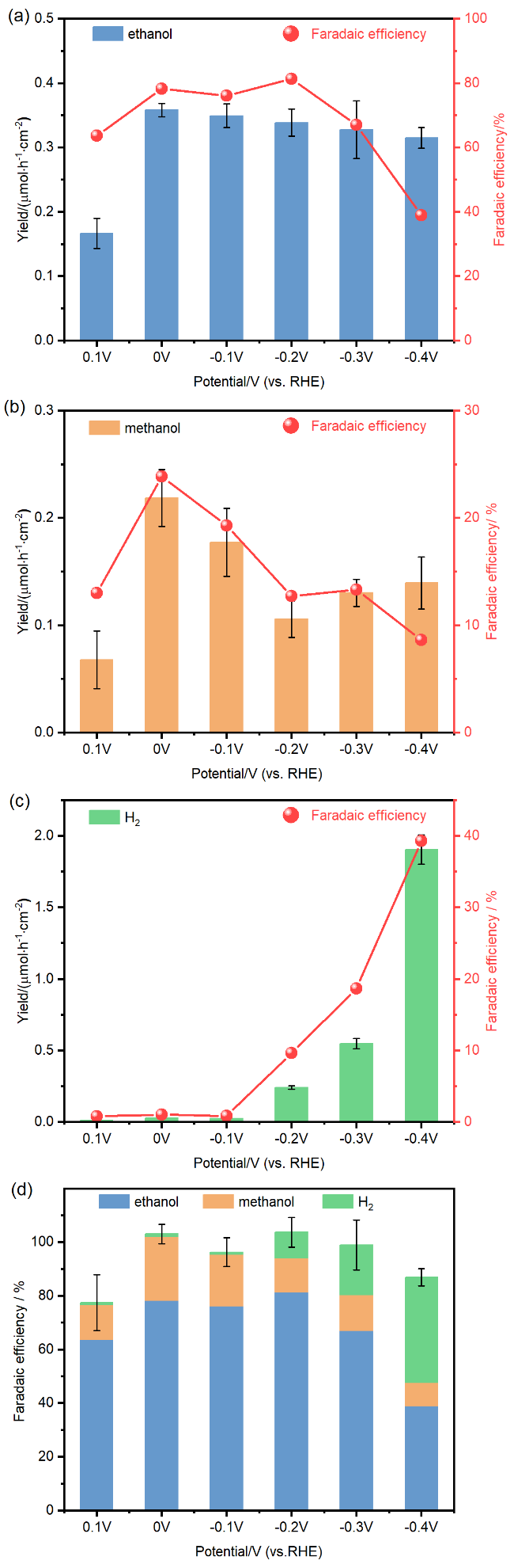
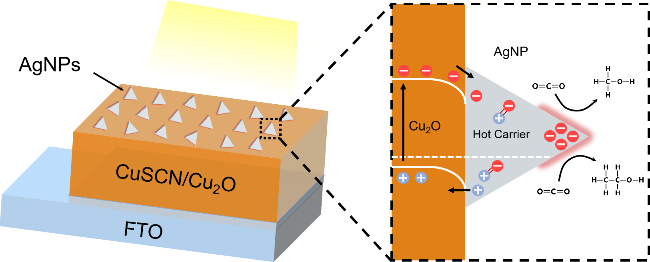
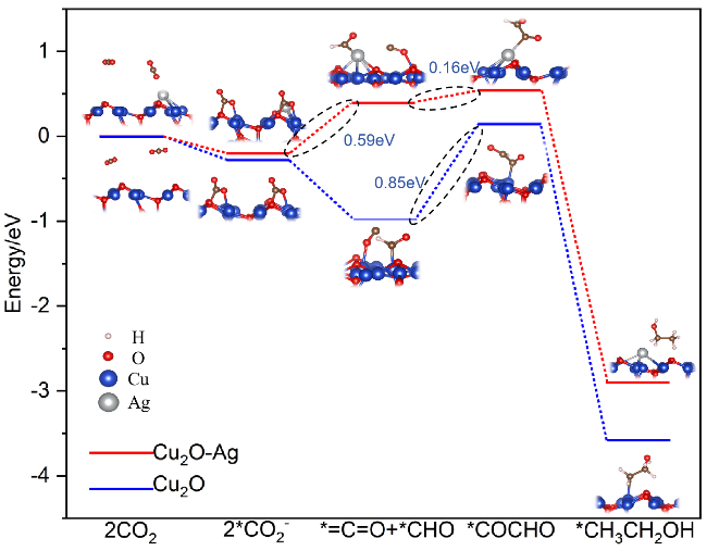
2 结果与讨论
2.1 LSPR纳米颗粒修饰光电阴极结构表征
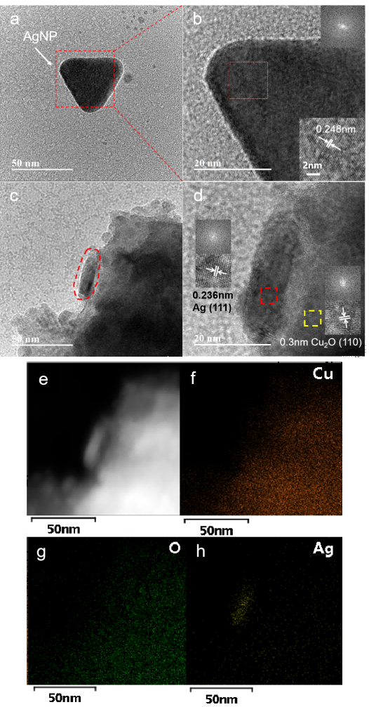
图1 (a)银纳米颗粒的TEM全貌图像; (b) AgNPs的TEM局部放大图像, 右上角插图是所选区域快速傅里叶变换图, 右下角显示AgNPs晶格间距; (c) Cu2O负载AgNPs (红色虚线区域)的TEM图像; (d) Cu2O/ AgNPs复合结构的局部放大TEM图像, 左、右插图分别对应Ag、Cu2O结构所选区域快速傅里叶变换图与晶格间距; (e~h)氧化亚铜负载银纳米颗粒EDS元素分布Figure 1 (a) TEM image of AgNPs; (b) magnified TEM image of AgNPs, with the inset in the upper right corner showing the fast Fourier transform (FFT) pattern of the selected area, and the lower right corner displaying the lattice spacing of the AgNPs; (c) TEM image of Cu2O loaded with AgNPs (red dashed area); (d) magnified TEM image of the Cu2O/AgNPs composite structure, with the left and right insets showing the FFT pattern and lattice spacing of the selected Ag and Cu2O regions, respectively; (e~h) EDS elemental distribution of silver nanoparticles supported on cuprous oxide |
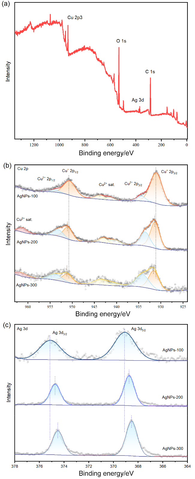
图3 (a) FTO/CuSCN/Cu2O/AgNPs光电阴极的XPS全谱图; 不同AgNPs负载量的FTO/CuSCN/Cu2O/AgNPs光电阴极XPS谱图对比: (b) Cu 2p轨道精细谱图; (c) Ag 3d轨道精细谱图Figure 3 (a) XPS survey spectrum of FTO/CuSCN/Cu2O/AgNPs photocathode; Comparison of XPS spectra of FTO/CuSCN/Cu2O/AgNPs photocathodes with different AgNPs loadings: (b) fine spectrum of Cu 2p orbital; (c) fine spectrum of Ag 3d orbital |
2.2 AgNPs负载光学特性测试
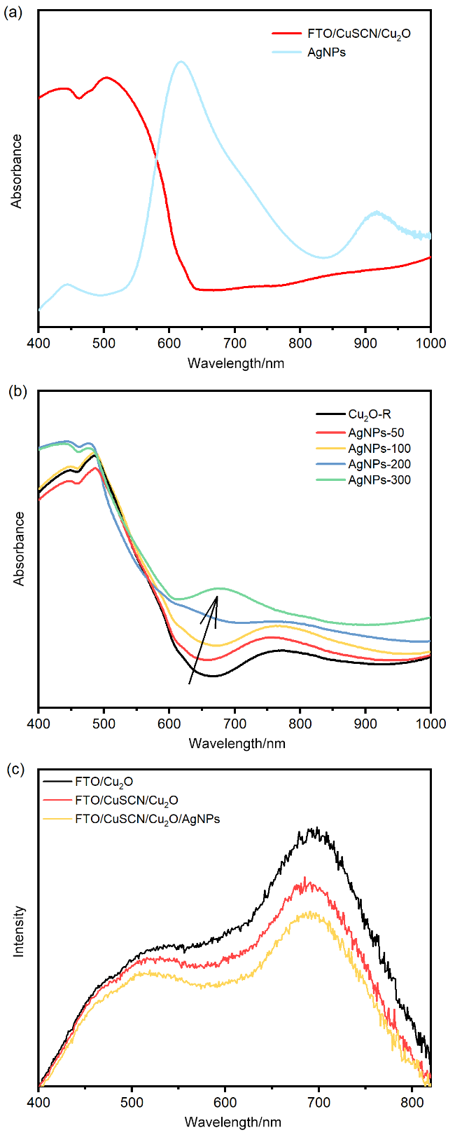
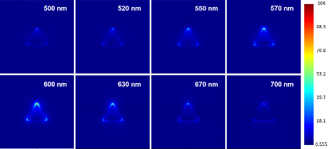
图4 (a) AgNPs溶液的光吸收特性; (b)不同AgNPs负载的复合光电阴极光吸收特性; (c) CuSCN改进与AgNPs负载修饰前后光电阴极的光致发光光谱Figure 4 (a) Optical absorption characteristics of AgNPs solution; (b) optical absorption characteristics of composite photocathodes with different AgNPs loadings; (c) PL of the photocathode before and after modification with CuSCN improvement and AgNPs loading. |