


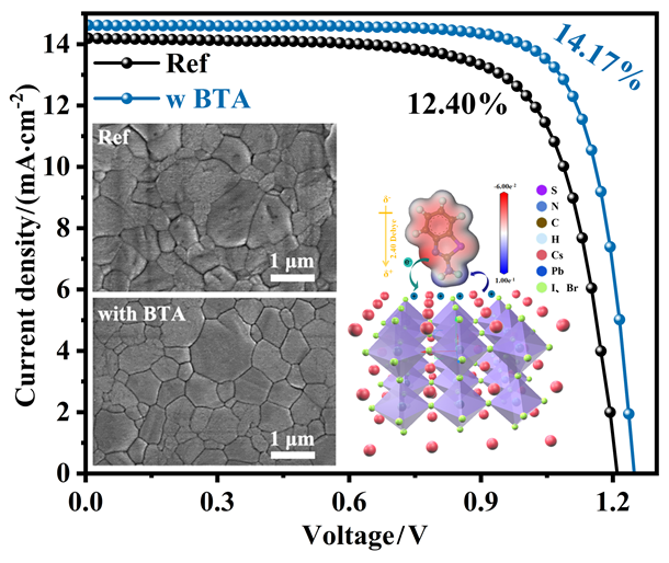
1 引言
2 结果与讨论
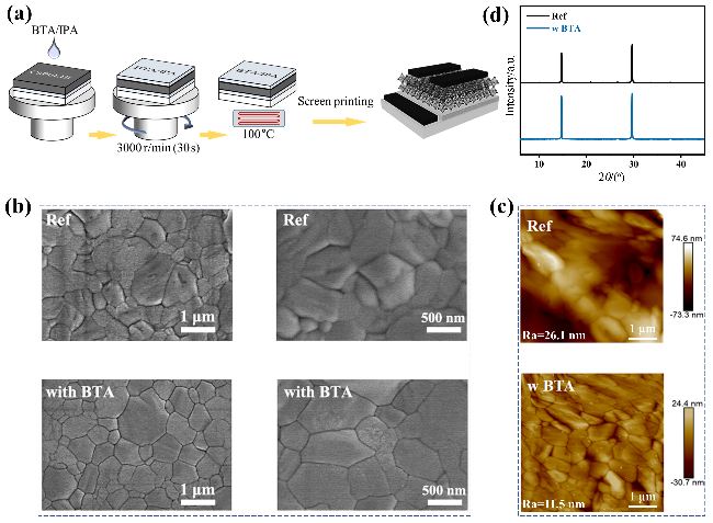
图1 (a) CsPbI2Br 薄膜上部界面的后处理工艺流程图; CsPbI2Br薄膜在经过BTA界面改性前后: (b) SEM图像; (c) AFM图像; (d) XRD图谱Figure 1 (a) CsPbI2Br film upper interface post-treatment process flow chart; CsPbI2Br perovskite films before and after BTA interface modification: (b) SEM images; (c) AFM images; (d) XRD patterns |
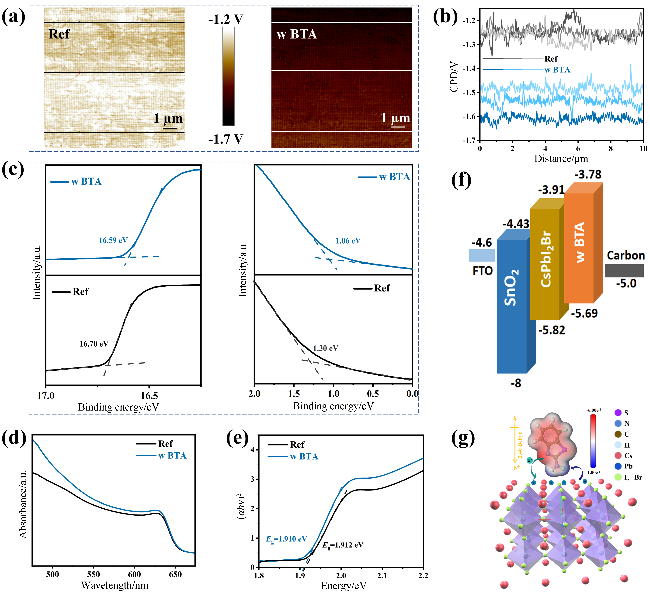
图3 BTA界面处理前后的CsPbI2Br薄膜: (a)表面电位分布图(KPFM); (b)相应区域的表面电位(或接触电位差)曲线; (c) UPS谱图; (d)紫外-可见光谱; (e) Tauc图; (f)器件中各功能层的能级排列; (g)表面偶极子的电荷转移和BTA排列Figure 3 CsPbI2Br perovskite films before and after BTA interface modification: (a) Surface potential profile (KPFM); (b) The surface potential (or contact potential difference) curve of the corresponding region; (c) UPS spectrum diagram; (d) UV-vis spectra; (e) Tauc diagram; (f) Energy level arrangement of each functional layer in PSCs; (g) charge transfer and BTA arrangement of surface dipoles |
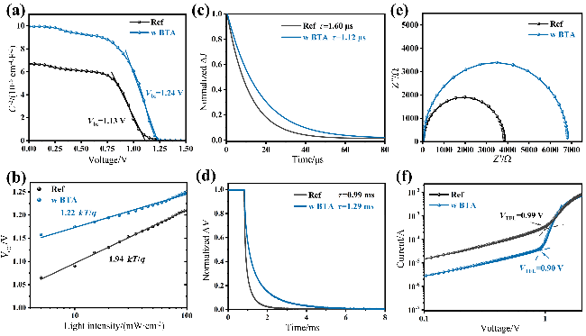
图4 原始装置与使用最佳浓度的BTA进行修饰后的装置: (a) M-S曲线; (b)光强度与开路电压关系曲线; (c) TPC衰减曲线; (d) TPV衰减曲线; (e) EIS曲线; (f) SCLC曲线Figure 4 Original device and device modified with optimal concentration of BTA: (a) M-S curve; (b) VOC light intensity dependence curve; (c) TPC attenuation curve; (d) TPV attenuation curve; (e) EIS curve; (f) SCLC curve |
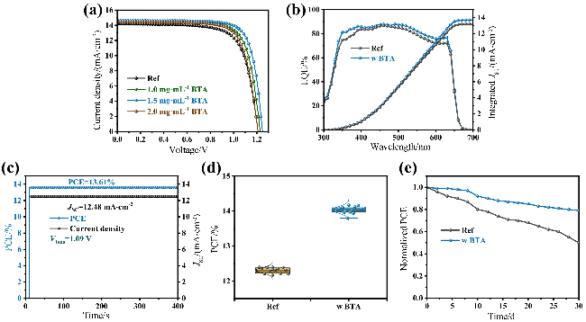


图5 原始器件与BTA修饰器件: (a) J-V曲线; (b) EQE-IPCE曲线; (c)最大功率点的稳态输出曲线; (d) PCE统计图; (e)器件的长期稳定性Figure 5 Original device and BTA-modified device: (a) J-V curve; (b) IPCE integration curve; (c) Steady-state output curve of maximum power point; (d) PCE statistical box diagram; (e) Long-term PCE stability of the device |