化学学报 ›› 2022, Vol. 80 ›› Issue (3): 395-422.DOI: 10.6023/A21110513 上一篇
综述
周静a, 田雪迎a,b, 王斌凯a,b, 张沙沙c, 刘宗豪a,*( ), 陈炜a,*()
投稿日期:2021-11-12
发布日期:2022-01-10
通讯作者:
刘宗豪, 陈炜
作者简介: |
周静, 2018年于中国地质大学(武汉)获应用化学系理学士学位.目前是华中科技大学武汉国家光电研究中心2018级博士研究生, 主要研究方向为反式钙钛矿太阳能电池的稳定性研究. |
 |
田雪迎, 2019年于济南大学新能源科学与工程学院获理学士学位. 目前是华中科技大学中欧清洁与可再生能源学院2019级硕士研究生, 主要研究方向为钙钛矿太阳能电池的封装和长期稳定性研究. |
 |
王斌凯, 2019年于河北大学质量技术监督学院获管理学学士学位. 目前是华中科技大学中欧清洁与可再生能源学院2019级硕士研究生, 主要研究方向为大面积钙钛矿太阳能电池的刮涂及模组制备研究. |
 |
刘宗豪, 副教授, 2011年于华中科技大学获理学士学位, 2016年于华中科技大学获博士学位. 2015年在美国洛杉矶加利福尼亚州访学交流. 2016至2017年在北京大学做研究助理. 2017至2019年在日本冲绳理工大学研究生院做博士后. 目前是华中科技大学武汉国家光电研究中心副教授, 主要从事有机无机杂化钙钛矿光电器件性能研究. |
 |
陈炜, 教授, 于清华大学材料科学与工程系获硕士和博士学位. 2008年2010年于香港科技大学化学系做博士后. 2014年至2015年于日本国际材料化学协会做访问学者. 目前是华中科技大学武汉国家光电研究中心教授, 主要从事纳米材料的合成、基础研究和应用以及新型太阳能电池(包括钙钛矿太阳能电池)半导体薄膜的研究. |
基金资助:
Jing Zhoua, Xueying Tiana,b, Binkai Wanga,b, Shasha Zhangc, Zonghao Liua(), Wei Chena()
Received:2021-11-12
Published:2022-01-10
Contact:
Zonghao Liu, Wei Chen
Supported by:文章分享
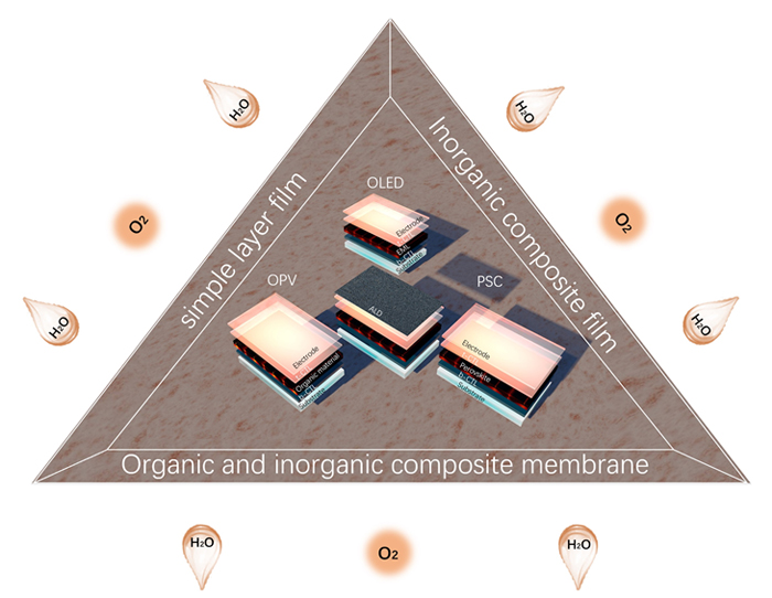
有机半导体光电器件在基础研究和工业应用方面进展迅速, 相关方向已经成为一个较为成熟的新兴领域. 然而, 这类器件中的关键有机材料存在对空气中的水、氧十分敏感的问题, 严重影响了器件的长期工作性能. 除了选择合适的传输层材料、界面层结构, 利用界面工程提高器件水氧耐受能力之外, 对器件进行可靠的封装是隔绝空气中水、氧的另一个有效手段. 原子层沉积(atomic layer deposition, ALD)是一种近乎完美的薄膜沉积封装技术, 这种技术所生长的薄膜具有独特的层-层(layer by layer)生长特性, 而且可以在低温下沉积出厚度可控、重复率高、均匀致密的薄膜, 使得该技术在半导体行业已经得到广泛应用. 在此, 我们将回顾ALD封装技术在有机发光二极管(organic light emitting diode, OLED)、有机太阳能电池(organic photovoltaics, OPV)和钙钛矿太阳能电池(perovskite solar cell, PSC)中的应用, 并进一步讨论现阶段应用于OLED的相对比较成熟的ALD封装技术, 及其对OPV和PSC封装的启示性意义.
周静, 田雪迎, 王斌凯, 张沙沙, 刘宗豪, 陈炜. 低温原子层沉积封装技术在OLED上的应用及对有机、钙钛矿太阳能电池封装的启示[J]. 化学学报, 2022, 80(3): 395-422.
Jing Zhou, Xueying Tian, Binkai Wang, Shasha Zhang, Zonghao Liu, Wei Chen. Application of Low Temperature Atomic Layer Deposition Packaging Technology in OLED and Its Implications for Organic and Perovskite Solar Cell Packaging[J]. Acta Chimica Sinica, 2022, 80(3): 395-422.


| Deposition temp./℃ | Structure | Thickness/nm | dyads | Test temp./℃ | Test temp. RH% | WVTR/ (g•m-2•d-1) | Bending radius/ cm | Bending cycle | WVTR change after bending/% | Ref. |
|---|---|---|---|---|---|---|---|---|---|---|
| 80 | Al2O3 | 25 | 1 | 85 | 85 | 4.50×10⁻⁴ | 1.5 | 1000 | 374% | [ |
| 80 | Al2O3/cyclohexane-plasma polymer/Al2O3 | 12.5/100/12.5 | 1 | 85 | 85 | 2.70×10⁻⁴ | 1.5 | 1000 | 101% | [ |
| 80 | Al2O3/Li(acac)/Al2O3 | 12.5/100/12.5 | 1 | 85 | 85 | 1.50×10⁻⁴ | 1.5 | 1000 | 131% | [ |
| 80 | Al2O3/TiMO/ Al2O3 | 12.5/100/12.5 | 1 | 85 | 85 | 1.70×10⁻⁴ | 1.5 | 1000 | 137% | [ |
| 120 | Al2O3/HfO2 | 2/2 | 9 | 38 | 100 | 6.00×10⁻⁶ | — | — | — | [ |
| 300 | Al2O3/HfO2 | 2/2 | 5 | 38 | 100 | 5.00×10⁻⁶ | — | — | — | [ |
| 80 | Al2O3/ 4MP | 3/0.6 | 3.5 | r.t. | r.t. | 2.32×10⁻⁷ | — | — | — | [ |
| 80 | Al2O3 | 50 | 1 | 85 | 85 | 3.10×10⁻⁴ | — | — | — | [ |
| 90 | Al2O3/alucone | 15/2.5 | 5.5 | 25 | 60 | 1.44×10⁻⁴ | — | — | — | [ |
| 80 | SAM/Al2O3/Ag | 40/8 | 1 | 38 | 100 | 5.00×10⁻⁵ | — | — | — | [ |
| 80 | Al2O3/15% C Al2O3 | 6.7/2.5 | 5 | 85 | 85 | 3.20×10⁻⁴ | 1.5 | 1000 | 186% | [ |
| 60 | parylene C/Al2O3 | 30/500 | 3 | 38 | 100 | 5.00×10⁻⁵ | — | — | — | [ |
| 80 | AMO / CYTOP | 100/2000 | 1 | 60 | 100 | 1.05×10⁻⁶ | — | — | — | [ |
| 80 | SAOLs/Al2O3 | 10.4/20.1 | 5 | r.t./25 | r.t./40 | 2.99×10⁻⁷ | — | — | — | [ |
| 80 | SAOLs/Al2O3 | 10.4/20.1 | 5 | 85 | 85 | 1.58×10⁻³ | — | — | — | [ |
| 40 | Al2O3 | 100 | 1 | 85 | 85 | 1.84×10⁻³ | — | — | — | [ |
| 80 | ZrO2 | 80 | 1 | 20 | 60 | 6.09×10⁻⁴ | — | — | — | [ |
| 40 | Al2O3 | 100 | 1 | 37.8 | 100 | 9.20×10⁻⁷ | — | — | — | [ |
| 70 | Al2O3/ZnO | 3/3 | 5 | 30 | 90 | 4.92×10⁻⁴ | — | — | — | [ |
| 70 | (Al2O3/ZnO nano-stratified stack)/S-H nanocomposite | 30/120 | 2.5 | 30 | 90 | 1.91×10⁻⁵ | 3 | 1000 | 212% | [ |
| 100 | Al2O3/ZrO2 | 10/10 | 5 | 50 | 50 | 3.97×10⁻⁴ | — | — | — | [ |
| 80 | AlOx/plasma polymer | 1/20 | 20 | 85 | 85 | 3.00×10⁻⁴ | 0.5 | 10000 | ≈100% | [ |
| 80 | Al2O3/TiO2 | 5/5 | 8 | 85 | 85 | 2.10×10⁻⁵ | — | — | — | [ |
| 60 | Al2O3/ZnO | 2/2 | 9 | 38 | 100 | 1.00×10⁻⁶ | — | — | — | [ |
| 50 | Al2O3/HfO2 | 2/2 | 9 | 38 | 100 | 3.50×10⁻⁶ | — | — | — | [ |
| 80 | Al2O3/MgO | 0.082/1.01 | 50/10 | 60 | 100 | 4.70×10⁻⁶ | — | — | — | [ |
| 75 | SiO2 | 70 | 1 | 37.8 | 100 | 7.73×10⁻³ | — | — | — | [ |
| 85 | MgO/S-H nanocomposite | 40/200 | 4.5 | 30 | 90 | 4.33×10⁻⁶ | — | — | — | [ |
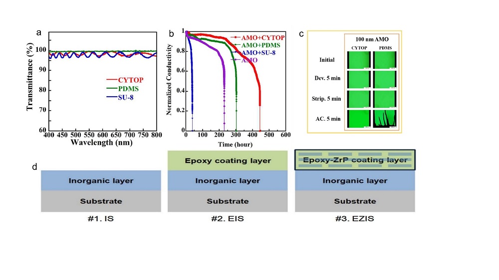
| 80 | NOA63/ZrO2/NOA63 | 16000/85/16000 | 1 | 20 | 50 | 9.00×10⁻⁵ | — | — | — | [ |
| 80 | ZrO2/NOA63 | 28/16000 | 2 | 20 | 60 | 1.27×10⁻⁴ | — | — | — | [ |
| 80 | ZrO2/zircone | 4/1 | 15 | 20 | 60 | 3.078×10⁻⁵ | — | — | — | [ |
| 70 | ZnO/Al2O3/MgO | 20/12/10 | 6 | 30 | 90 | 2.06×10⁻⁶ | 0.5 | — | 10-6 | [ |
| 70 | Al2O3/S-H nanocomposite | 60/2000 | 3 | 30 | 90 | 1.11×10⁻⁶ | 1 | 100 | — | [ |
| Deposition temp./℃ | Structure | Thickness/nm | dyads | Test temp./℃ | Test temp. RH% | WVTR/ (g•m-2•d-1) | Bending radius/ cm | Bending cycle | WVTR change after bending/% | Ref. |
|---|---|---|---|---|---|---|---|---|---|---|
| 80 | Al2O3 | 25 | 1 | 85 | 85 | 4.50×10⁻⁴ | 1.5 | 1000 | 374% | [ |
| 80 | Al2O3/cyclohexane-plasma polymer/Al2O3 | 12.5/100/12.5 | 1 | 85 | 85 | 2.70×10⁻⁴ | 1.5 | 1000 | 101% | [ |
| 80 | Al2O3/Li(acac)/Al2O3 | 12.5/100/12.5 | 1 | 85 | 85 | 1.50×10⁻⁴ | 1.5 | 1000 | 131% | [ |
| 80 | Al2O3/TiMO/ Al2O3 | 12.5/100/12.5 | 1 | 85 | 85 | 1.70×10⁻⁴ | 1.5 | 1000 | 137% | [ |
| 120 | Al2O3/HfO2 | 2/2 | 9 | 38 | 100 | 6.00×10⁻⁶ | — | — | — | [ |
| 300 | Al2O3/HfO2 | 2/2 | 5 | 38 | 100 | 5.00×10⁻⁶ | — | — | — | [ |
| 80 | Al2O3/ 4MP | 3/0.6 | 3.5 | r.t. | r.t. | 2.32×10⁻⁷ | — | — | — | [ |
| 80 | Al2O3 | 50 | 1 | 85 | 85 | 3.10×10⁻⁴ | — | — | — | [ |
| 90 | Al2O3/alucone | 15/2.5 | 5.5 | 25 | 60 | 1.44×10⁻⁴ | — | — | — | [ |
| 80 | SAM/Al2O3/Ag | 40/8 | 1 | 38 | 100 | 5.00×10⁻⁵ | — | — | — | [ |
| 80 | Al2O3/15% C Al2O3 | 6.7/2.5 | 5 | 85 | 85 | 3.20×10⁻⁴ | 1.5 | 1000 | 186% | [ |
| 60 | parylene C/Al2O3 | 30/500 | 3 | 38 | 100 | 5.00×10⁻⁵ | — | — | — | [ |
| 80 | AMO / CYTOP | 100/2000 | 1 | 60 | 100 | 1.05×10⁻⁶ | — | — | — | [ |
| 80 | SAOLs/Al2O3 | 10.4/20.1 | 5 | r.t./25 | r.t./40 | 2.99×10⁻⁷ | — | — | — | [ |
| 80 | SAOLs/Al2O3 | 10.4/20.1 | 5 | 85 | 85 | 1.58×10⁻³ | — | — | — | [ |
| 40 | Al2O3 | 100 | 1 | 85 | 85 | 1.84×10⁻³ | — | — | — | [ |
| 80 | ZrO2 | 80 | 1 | 20 | 60 | 6.09×10⁻⁴ | — | — | — | [ |
| 40 | Al2O3 | 100 | 1 | 37.8 | 100 | 9.20×10⁻⁷ | — | — | — | [ |
| 70 | Al2O3/ZnO | 3/3 | 5 | 30 | 90 | 4.92×10⁻⁴ | — | — | — | [ |
| 70 | (Al2O3/ZnO nano-stratified stack)/S-H nanocomposite | 30/120 | 2.5 | 30 | 90 | 1.91×10⁻⁵ | 3 | 1000 | 212% | [ |
| 100 | Al2O3/ZrO2 | 10/10 | 5 | 50 | 50 | 3.97×10⁻⁴ | — | — | — | [ |
| 80 | AlOx/plasma polymer | 1/20 | 20 | 85 | 85 | 3.00×10⁻⁴ | 0.5 | 10000 | ≈100% | [ |
| 80 | Al2O3/TiO2 | 5/5 | 8 | 85 | 85 | 2.10×10⁻⁵ | — | — | — | [ |
| 60 | Al2O3/ZnO | 2/2 | 9 | 38 | 100 | 1.00×10⁻⁶ | — | — | — | [ |
| 50 | Al2O3/HfO2 | 2/2 | 9 | 38 | 100 | 3.50×10⁻⁶ | — | — | — | [ |
| 80 | Al2O3/MgO | 0.082/1.01 | 50/10 | 60 | 100 | 4.70×10⁻⁶ | — | — | — | [ |
| 75 | SiO2 | 70 | 1 | 37.8 | 100 | 7.73×10⁻³ | — | — | — | [ |
| 85 | MgO/S-H nanocomposite | 40/200 | 4.5 | 30 | 90 | 4.33×10⁻⁶ | — | — | — | [ |
| 80 | NOA63/ZrO2/NOA63 | 16000/85/16000 | 1 | 20 | 50 | 9.00×10⁻⁵ | — | — | — | [ |
| 80 | ZrO2/NOA63 | 28/16000 | 2 | 20 | 60 | 1.27×10⁻⁴ | — | — | — | [ |
| 80 | ZrO2/zircone | 4/1 | 15 | 20 | 60 | 3.078×10⁻⁵ | — | — | — | [ |
| 70 | ZnO/Al2O3/MgO | 20/12/10 | 6 | 30 | 90 | 2.06×10⁻⁶ | 0.5 | — | 10-6 | [ |
| 70 | Al2O3/S-H nanocomposite | 60/2000 | 3 | 30 | 90 | 1.11×10⁻⁶ | 1 | 100 | — | [ |
| ALD cycles | O3-Al2O3 | H2O-Al2O3 | |||||
|---|---|---|---|---|---|---|---|
| ηinitial | η350 h | %ηretention | ηinitial | η350 h | %ηretention | ||
| 90 | 2.36 | 0.82 | 35 | 2.50 | 0.01 | 0.4 | |
| 120 | 2.47 | 1.13 | 46 | 2.76 | 0.05 | 2 | |
| 150 | 2.52 | 1.61 | 64 | 2.64 | 0.74 | 28 | |
| 210 | 2.69 | 2.35 | 87 | 2.78 | 0.91 | 33 | |


| Device structure | Deposition temperature/℃ | WVTR/ (g•m-2•d-1) | PCE/% | Aging condition and stablity tests | Ref. |
|---|---|---|---|---|---|
| ITO/PEDOT:PSS/MAPbI3/PCBM/ ALD ZnO/Ag NWs/50 nm ALD Al2O3 coated PET | 100 | 9×10⁻⁴ | 10.55 | being exposed to ambience (30 ℃, 65% relative humidity) for more than 40 d | [ |
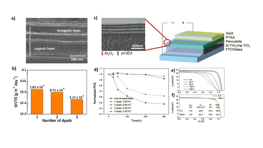
| FTO/bl-TiO2/mp-TiO2/(FAPbI3)0.87- (MAPbBr3)0.13/PTAA/Au/ALD Al2O3/pV3D3 | 60 | 1×10⁻⁴ | 18.2±1.3 | maintained 97% of its original efficiency after 300 h of exposure at 50 ℃ and 50% RH. | [ |
| FTO/ALD-NiO/Cs0.05MA0.95PbI3/ PCBM/BCP/ALD-AZO/Ag /50 nm ALD Al2O3 | 100 | — | 18.4 | maintaining 86.7% of the initial PCE under continuous1 Sun illumination at 85 ℃ in ambient air with constant near maximum power point over 500 h | [ |
| ITO/NIO/CH3NH3PbI3/PC61BM/ALD TiO2/Ag/60 nm ALD Al2O3 | 60 | — | — | 93% of the initial PCE remained after being stored in ambient for a thousand hours | [ |
| FTO/bl-TiO2/mp-TiO2/MAPbI3/Spiro-OMeTAD/Au/16 nm ALD Al2O3 | 60 | — | 17.4 | exhibited a final PCE of 12.4% after more than 2250 h of storage underambient conditions (from original PCE=16.4%) | [ |
| FTO/bl-TiO2/mp-TiO2/(FAPbI3)0.85- (MAPbBr3)0.15/PTAA/Au/50 nm Al2O3 | 95 | 1.84×10⁻² | 15.3 | with less than 4% drop in PCE after 7500 h (>10 months) of exposure to 50%RH under room temperature. | [ |
| ITO/SnO2/MAPbI3/Spiro-MeOTD/Ag/Alucone/ALD Al2O3 | 50 | 1.3×10⁻⁵ | 17.01 | at 80% relative humidity and 30 ℃ for over 2000 h while preserving 96% of its initial performance | [ |
| FTO/SnO2/(FA0.83MA0.17)0.95Cs0.05- PbI2.5Br0.5/Spiro-OMeTAD/Au/300 cycles ALD Al2O3 | 75 | — | 19.4 | retaining 84% of its initial efficiency by the end of 300 d stored in ambient conditions | [ |
| Device structure | Deposition temperature/℃ | WVTR/ (g•m-2•d-1) | PCE/% | Aging condition and stablity tests | Ref. |
|---|---|---|---|---|---|
| ITO/PEDOT:PSS/MAPbI3/PCBM/ ALD ZnO/Ag NWs/50 nm ALD Al2O3 coated PET | 100 | 9×10⁻⁴ | 10.55 | being exposed to ambience (30 ℃, 65% relative humidity) for more than 40 d | [ |
| FTO/bl-TiO2/mp-TiO2/(FAPbI3)0.87- (MAPbBr3)0.13/PTAA/Au/ALD Al2O3/pV3D3 | 60 | 1×10⁻⁴ | 18.2±1.3 | maintained 97% of its original efficiency after 300 h of exposure at 50 ℃ and 50% RH. | [ |
| FTO/ALD-NiO/Cs0.05MA0.95PbI3/ PCBM/BCP/ALD-AZO/Ag /50 nm ALD Al2O3 | 100 | — | 18.4 | maintaining 86.7% of the initial PCE under continuous1 Sun illumination at 85 ℃ in ambient air with constant near maximum power point over 500 h | [ |
| ITO/NIO/CH3NH3PbI3/PC61BM/ALD TiO2/Ag/60 nm ALD Al2O3 | 60 | — | — | 93% of the initial PCE remained after being stored in ambient for a thousand hours | [ |
| FTO/bl-TiO2/mp-TiO2/MAPbI3/Spiro-OMeTAD/Au/16 nm ALD Al2O3 | 60 | — | 17.4 | exhibited a final PCE of 12.4% after more than 2250 h of storage underambient conditions (from original PCE=16.4%) | [ |
| FTO/bl-TiO2/mp-TiO2/(FAPbI3)0.85- (MAPbBr3)0.15/PTAA/Au/50 nm Al2O3 | 95 | 1.84×10⁻² | 15.3 | with less than 4% drop in PCE after 7500 h (>10 months) of exposure to 50%RH under room temperature. | [ |
| ITO/SnO2/MAPbI3/Spiro-MeOTD/Ag/Alucone/ALD Al2O3 | 50 | 1.3×10⁻⁵ | 17.01 | at 80% relative humidity and 30 ℃ for over 2000 h while preserving 96% of its initial performance | [ |
| FTO/SnO2/(FA0.83MA0.17)0.95Cs0.05- PbI2.5Br0.5/Spiro-OMeTAD/Au/300 cycles ALD Al2O3 | 75 | — | 19.4 | retaining 84% of its initial efficiency by the end of 300 d stored in ambient conditions | [ |
| Material | Temperature/℃ | WVTR/ (g•m-2•d-1) | Jsc/ (mA•cm-2) | PCE/% | Lifetime | Cycle | Thickness/nm | Ref. |
|---|---|---|---|---|---|---|---|---|
| ITO/PEDOT:PSS/ Polymer:PCBM/Ca/Al | 80 | — | 5.31 | 1.93 | 300 h/72% | 1000 | 100(Al2O3) | [ |
| ITO/PEDOT:PSS/ rrP3HT:PC70BM/Yb/Al | 70 | — | — | — | 250 min/95% | 3000 | 330(Al2O3) | [ |
| ITO/PEIE/P3HT:ICBA/ MoO3/Ag | 30 | — | 9 | 3 | >1400 h/88% | — | 10(TiO2)/10(Al2O3)/ 400(SiNx)/30(Al2O3)/ 10(TiO2) | [ |
| ITO/PEDOT:PSS/ P3HT:PCBM/AlOx/Pt | 100 | — | 7 | 2.9 | >2000 h/30% | 999 | ≤100 | [ |
| OPV | 90 | 1.29×10⁻⁵ | — | — | — | — | 500(pV4D4)/35(Al2O3)/200(pV4D4)/35(Al2O3)/200(pV4D4)/35(Al2O3) | [ |
| ITO/PEDOT:PSS/ P3HT:PCBM/Al | 100 | <5×10⁻⁴ | 8.3 | 3.1 | >450 h/50% | 480 | 27(AlOx/HfOx cycle 30) | [ |
| ITO/MoOx/ClAlPc/ ClAlPc:C60/C60/BCP/Ag | 100 | <5×10⁻⁴ | — | 1.7 | >1200 h/10% | 480 | 27(AlOx/HfOx cycle 30) | [ |
| ITO/PEDOT:PSS/ P3HT:PCBM/Al | 140 | — | 9.15 | 2.7 | 500 h/80% | 210 | 18(Al2O3) | [ |
| ITO/PEDOT:PSS/ P3HT:PCBM/Al | 140 | — | 9.98 | 3.66 | 640 h/50% | 104 | 26(Al2O3/HfO2 cycle 52)+UV-curable epoxy resin film | [ |
| ITO/pentacene/C60/ BCP/Al | 100 | — | 11.1 | 2.8 | 6145 h/94% | — | 200(Al2O3) | [ |
| [1] |
Kojima, A.; Teshima, K.; Shirai, Y.; Miyasaka, T. J. Am. Chem. Soc. 2009, 131, 6050.
doi: 10.1021/ja809598r |
| [2] |
Zhao, B.; Bai, S.; Kim, V.; Lamboll, R.; Shivanna, R.; Auras, F.; Richter, J. M.; Yang, L.; Dai, L.; Alsari, M.; She, X.-J.; Liang, L.; Zhang, J.; Lilliu, S.; Gao, P.; Snaith, H. J.; Wang, J.; Greenham, N. C.; Friend, R. H.; Di, D. Nat Photonics 2018, 12, 783.
doi: 10.1038/s41566-018-0283-4 |
| [3] |
Yuan, J.; Zhang, Y.; Zhou, L.; Zhang, G.; Yip, H.-L.; Lau, T.-K.; Lu, X.; Zhu, C.; Peng, H.; Johnson, P. A.; Leclerc, M.; Cao, Y.; Ulanski, J.; Li, Y.; Zou, Y. Joule 2019, 3, 1140.
doi: 10.1016/j.joule.2019.01.004 |
| [4] |
Lee, M. M.; Teuscher, J.; Miyasaka, T.; Murakami, T. N.; Snaith, H. J. Science 2012, 338, 643.
doi: 10.1126/science.1228604 |
| [5] |
Hu, X.-M.; Zhong, C.-X.; Li, X.-Y.; Jia, X.; Wei, Y.; Xie, L.-H. Acta Chim. Sinica 2021, 79, 953. (in Chinese)
doi: 10.6023/A21050196 |
|
(胡鑫明, 钟春晓, 李晓艳, 贾雄, 魏颖, 解令海, 化学学报, 2021, 79, 953.)
doi: 10.6023/A21050196 |
|
| [6] |
Miao, J.-H.; Ding, Z.-C.; Liu, J.; Wang, L.-X. Acta Chim. Sinica 2021, 79, 545. (in Chinese)
doi: 10.6023/A20120589 |
|
(苗俊辉, 丁自成, 刘俊, 王利祥, 化学学报, 2021, 79, 545.)
doi: 10.6023/A20120589 |
|
| [7] |
Zhou, M.; Li, J.; Chneg, J.; Ge, C.-W.; Cheng, T.-Y.; Gao, X.-K. Chin. J. Org. Chem. 2021, 41, 4400. (in Chinese)
doi: 10.6023/cjoc202105023 |
|
(周敏, 李晶, 程杰, 葛从伍, 程探宇, 高希珂, 有机化学, 2021, 41, 4400.)
doi: 10.6023/cjoc202105023 |
|
| [8] |
Bian, Y.-S.; Liu, K.; Guo, Y.-L.; Liu, Y.-Q. Acta Chim. Sinica 2020, 78, 848. (in Chinese)
doi: 10.6023/A20050197 |
|
(边洋爽, 刘凯, 郭云龙, 刘云圻, 化学学报, 2020, 78, 848.)
doi: 10.6023/A20050197 |
|
| [9] |
Hou, B.; Li, J.; Xin, Z.-H.; Yang, X.-D.; Gao, H.-L.; Peng, P.-Z.; Gao, X.-K. Acta Chim. Sinica 2020, 78, 788. (in Chinese)
doi: 10.6023/A20050161 |
|
(侯斌, 李晶, 辛涵申, 杨笑迪, 高洪磊, 彭培珍, 高希珂, 化学学报, 2020, 78, 788.)
doi: 10.6023/A20050161 |
|
| [10] |
Liu, H.; Zhang, X.-F.; Cheng, J.-Z.; Ye, D.-D.; Chen, L.; Wen, H.-R.; Liu, S.-Y. Chin. J. Org. Chem. 2020, 40, 831. (in Chinese)
doi: 10.6023/cjoc201910042 |
|
(刘慧, 张小凤, 程敬招, 叶东鼐, 陈龙, 温和瑞, 刘诗咏, 有机化学, 2020, 40, 831.)
doi: 10.6023/cjoc201910042 |
|
| [11] |
Cai, J.-F.; Jiang, H.; Cui, Z.-H.; Chen, W.-G. Chin. J. Org. Chem. 2020, 40, 351. (in Chinese)
|
|
(蔡金芳, 江华, 崔志华, 陈维国, 有机化学, 2020, 40, 351.)
doi: 10.6023/cjoc201909022 |
|
| [12] |
Dai, X.-X.; Cheng, X.-D.; Kan, Z.-P.; Xiao, Z.-Y.; Duan, T.-N.; Hu, C.; Lu, S.-R. Chin. J. Org. Chem. 2020, 40, 4031. (in Chinese)
doi: 10.6023/cjoc202005023 |
|
(戴学新, 成晓东, 阚志鹏, 肖泽云, 段泰男, 胡超, 陆仕荣, 有机化学, 2020, 40, 4031.)
doi: 10.6023/cjoc202005023 |
|
| [13] |
Jiang, D.-N.; Yan, K.-R.; Li, C.-Z. Acta Chim. Sinica 2020, 78, 1287. (in Chinese)
doi: 10.6023/A20080342 |
|
(蒋丹妮, 严康荣, 李昌治, 化学学报, 2020, 78, 1287.)
doi: 10.6023/A20080342 |
|
| [14] |
Li, T.-F.; Zhan, X.-W. Acta Chim. Sinica 2021, 79, 257 (In Chinese).
doi: 10.6023/A20110502 |
|
(李腾飞, 占肖卫, 化学学报, 2021, 79, 257.)
doi: 10.6023/A20110502 |
|
| [15] |
Park, S.; Yun, W. M.; Kim, L. H.; Park, S.; Kim, S. H.; Park, C. E. Org. Electron. 2013, 14, 3385.
doi: 10.1016/j.orgel.2013.09.045 |
| [16] |
Cheng, P.; Zhan, X. Chem. Soc. Rev. 2016, 45, 2544.
doi: 10.1039/c5cs00593k pmid: 26890341 |
| [17] |
Norrman, K.; Gevorgyan, S. A.; Krebs, F. C. ACS Appl. Mater. Interfaces 2009, 1, 102.
doi: 10.1021/am800039w |
| [18] |
Fu, Q.; Tang, X.; Huang, B.; Hu, T.; Tan, L.; Chen, L.; Chen, Y. Adv. Sci. (Weinh) 2018, 5, 1700387.
|
| [19] |
Yang, D.; Yang, Y. q.; Duan, Y.; Chen, P.; Zang, C. L.; Xie, Y.; Liu, D. M.; Wang, X.; Duan, Y. H.; Sun, F. B.; Gao, Q.; Xue, K. W. ECS Solid State Lett. 2013, 2, R31.
doi: 10.1149/2.007309ssl |
| [20] |
Eperon, G. E.; Habisreutinger, S. N.; Leijtens, T.; Bruijnaers, B. J.; van Franeker, J. J.; deQuilettes, D. W.; Pathak, S.; Sutton, R. J.; Grancini, G.; Ginger, D. S.; Janssen, R. A. J.; Petrozza, A.; Snaith, H. J. ACS Nano 2015, 9, 9380.
doi: 10.1021/acsnano.5b03626 pmid: 26247197 |
| [21] |
Wu, Z.; Bai, S.; Xiang, J.; Yuan, Z.; Yang, Y.; Cui, W.; Gao, X.; Liu, Z.; Jin, Y.; Sun, B. Nanoscale 2014, 6, 10505.
doi: 10.1039/C4NR03181D |
| [22] |
Kimura, M.; Kuwano, S.; Sawaki, Y.; Fujikawa, H.; Noda, K.; Taga, Y.; Takagi, K. J. Mater. Chem. 2005, 15, 2393.
doi: 10.1039/b502268a |
| [23] |
Ke, W.; Fang, G.; Liu, Q.; Xiong, L.; Qin, P.; Tao, H.; Wang, J.; Lei, H.; Li, B.; Wan, J.; Yang, G.; Yan, Y. J. Am. Chem. Soc. 2015, 137, 6730.
doi: 10.1021/jacs.5b01994 |
| [24] |
Bolink, H. J.; Coronado, E.; Repetto, D.; Sessolo, M.; Barea, E. M.; Bisquert, J.; Garcia-Belmonte, G.; Prochazka, J.; Kavan, L. Adv. Funct. Mater. 2008, 18, 145.
doi: 10.1002/adfm.v18:1 |
| [25] |
Wöhrle, D.; Meissner, D. Adv. Mater. 1991, 3, 129.
doi: 10.1002/adma.19910030303 |
| [26] |
Smith, I. C.; Hoke, E. T.; Solis-Ibarra, D.; McGehee, M. D.; Karunadasa, H. I. Angew. Chem. Int. Ed. 2014, 53, 11232.
doi: 10.1002/anie.201406466 |
| [27] |
Zhou, H.; Chen, Q.; Li, G.; Luo, S.; Song, T.-b.; Duan, H.-S.; Hong, Z.; You, J.; Liu, Y.; Yang, Y. Science 2014, 345, 542.
doi: 10.1126/science.1254050 |
| [28] |
Zhang, J.; Hu, Z.; Huang, L.; Yue, G.; Liu, J.; Lu, X.; Hu, Z.; Shang, M.; Han, L.; Zhu, Y. Chem. Commun. (Camb) 2015, 51, 7047.
doi: 10.1039/C5CC00128E |
| [29] |
Weerasinghe, H. C.; Dkhissi, Y.; Scully, A. D.; Caruso, R. A.; Cheng, Y.-B. Nano Energy 2015, 18, 118.
doi: 10.1016/j.nanoen.2015.10.006 |
| [30] |
Shi, L.; Bucknall, M. P.; Young, T. L.; Zhang, M.; Hu, L.; Bing, J.; Lee, D. S.; Kim, J.; Wu, T.; Takamure, N.; McKenzie, D. R.; Huang, S.; Green, M. A.; Ho-Baillie, A. W. Y. Science 2020, 368, 1328.
|
| [31] |
Han, Y.; Meyer, S.; Dkhissi, Y.; Weber, K.; Pringle, J. M.; Bach, U.; Spiccia, L.; Cheng, Y.-B. J. Mater. Chem. A 2015, 3, 8139.
doi: 10.1039/C5TA00358J |
| [32] |
Dong, Q.; Liu, F.; Wong, M. K.; Tam, H. W.; Djurisic, A. B.; Ng, A.; Surya, C.; Chan, W. K.; Ng, A. M. ChemSusChem 2016, 9, 2597.
doi: 10.1002/cssc.201600868 pmid: 27504719 |
| [33] |
Cheacharoen, R.; Boyd, C. C.; Burkhard, G. F.; Leijtens, T.; Raiford, J. A.; Bush, K. A.; Bent, S. F.; McGehee, M. D. Sustain. Energ. Fuels 2018, 2, 2398.
doi: 10.1039/C8SE00250A |
| [34] |
Satoh, R.-i.; Ro, T.; Heo, C.-J.; Lee, G. H.; Xianyu, W.; Park, Y.; Park, J.; Lim, S.-J.; Leem, D.-S.; Bulliard, X.; Kim, Y.; Bae, K.; Yang, W.-Y.; Park, K.-B.; Jin, Y. W.; Lee, S. Org. Electron. 2017, 41, 259.
doi: 10.1016/j.orgel.2016.11.013 |
| [35] |
Michels, J. J.; Peter, M.; Salem, A.; van Remoortere, B.; van den Brand, J. J. Mater. Chem. C 2014, 2, 5759.
doi: 10.1039/c4tc00707g |
| [36] |
Tranchida, D.; Piccarolo, S.; Soliman, M. Macromolecules 2006, 39, 4547.
doi: 10.1021/ma052727j |
| [37] |
Bernardi, A.; Macko, J.; Po, R.; Mahony, A.; Scudo, P.; Bulovic, V. Sol. Energy Mater. Sol. Cells 2013, 10, 1.
doi: 10.1016/0165-1633(84)90002-9 |
| [38] |
Kim, B. J.; Kim, D. H.; Kang, S. Y.; Ahn, S. D.; Im, S. G. J. Appl. Polym. Sci. 2014, 131, 40030.
|
| [39] |
Yang, C.; Bi, H.; Wan, D.; Huang, F.; Xie, X.; Jiang, M. J. Mater. Chem. A 2013, 1, 770.
doi: 10.1039/C2TA00234E |
| [40] |
Zhang, C.-X.; Song, G.-P.; Sun, Y.; Zhao, Y.-J.; He, X.-D. Mater. Rev. 2012, 26(S2), 124. (in Chinese)
|
|
(张传鑫, 宋广平, 孙跃, 赵轶杰, 赫晓东, 材料导报, 2012, 26(S2), 124.)
|
|
| [41] |
Sang, R.; Zhang, H.; Long, L.; Hua, Z.; Yu, J.; Wei, B.; Wu, X.; Feng, T.; Zhang, J. 2011 12th International Conference on Electronic Packaging Technology and High Density Packaging, IEEE, Shanghai, 2011, pp. 1-4.
|
| [42] |
Ono, S.; Häusermann, R.; Chiba, D.; Shimamura, K.; Ono, T.; Batlogg, B. Appl. Phys. Lett. 2014, 104, 013307.
doi: 10.1063/1.4860998 |
| [43] |
Chen, T.; Xue, Y.; Roy, A. K.; Dai, L. ACS Nano 2014, 8, 1039.
doi: 10.1021/nn405939w pmid: 24350978 |
| [44] |
Kukli, K.; Ritala, M.; Leskelä, M. Chem. Vap. Deposition 2000, 6, 297.
doi: 10.1002/(ISSN)1521-3862 |
| [45] |
George, S. M. Chem. Rev. 2010, 110, 111.
doi: 10.1021/cr900056b |
| [46] |
Ghazaryan, L.; Kley, E. B.; Tünnermann, A.; Szeghalmi, A. Nanotechnology 2016, 27, 255603.
doi: 10.1088/0957-4484/27/25/255603 pmid: 27176497 |
| [47] |
Koushik, D.; Verhees, W. J. H.; Kuang, Y.; Veenstra, S.; Zhang, D.; Verheijen, M. A.; Creatore, M.; Schropp, R. E. I. Energ. Environ. Sci. 2017, 10, 91.
doi: 10.1039/C6EE02687G |
| [48] |
Khalily, M. A.; Patil, B.; Yilmaz, E.; Uyar, T. Nanoscale Adv. 2019, 1, 1224.
doi: 10.1039/C8NA00330K |
| [49] |
Donders, M. E.; Knoops, H. C. M.; Kessels, W. M. M.; Notten, P. H. L. J. Power Sources 2012, 203, 72.
doi: 10.1016/j.jpowsour.2011.12.020 |
| [50] |
Hyde, G. K.; McCullen, S. D.; Jeon, S.; Stewart, S. M.; Jeon, H.; Loboa, E. G.; Parsons, G. N. Biomed. Mater. 2009, 4, 025001.
doi: 10.1088/1748-6041/4/2/025001 |
| [51] |
Leskelä, M.; Ritala, M. Thin Solid Films 2002, 409, 138.
doi: 10.1016/S0040-6090(02)00117-7 |
| [52] |
Hao, H.; Chen, X.; Li, Z.; Shen, Y.; Wang, H.; Zhao, Y.; Huang, R.; Liu, T.; Liang, J.; An, Y.; Peng, Q.; Ding, S. J. Semicond. 2019, 40, 012806.
doi: 10.1088/1674-4926/40/1/012806 |
| [53] |
Mackus, A. J. M.; Schneider, J. R.; MacIsaac, C.; Baker, J. G.; Bent, S. F. Chem. Mater. 2019, 31, 1142.
doi: 10.1021/acs.chemmater.8b02878 |
| [54] |
Lee, S.; Han, J.-H.; Lee, S.-H.; Baek, G.-H.; Park, J.-S. JOM 2018, 71, 197.
doi: 10.1007/s11837-018-3150-3 |
| [55] |
Seo, S.; Jeong, S.; Park, H.; Shin, H.; Park, N. G. Chem. Commun. (Camb) 2019, 55, 2403.
doi: 10.1039/C8CC09578G |
| [56] |
Zhou, B.; Liu, M.; Wen, Y.; Li, Y.; Chen, R. Opto-Electron. Adv. 2020, 3, 19004301.
doi: 10.29026/oea.2020.190043 |
| [57] |
Hossain, M. A.; Khoo, K. T.; Cui, X.; Poduval, G. K.; Zhang, T.; Li, X.; Li, W. M.; Hoex, B. Nano Mater. Sci. 2020, 2, 204.
|
| [58] |
Lu, Q.; Yang, Z.; Meng, X.; Yue, Y.; Ahmad, M. A.; Zhang, W.; Zhang, S.; Zhang, Y.; Liu, Z.; Chen, W. Adv. Funct. Mater. 2021, 31, 2100151.
doi: 10.1002/adfm.v31.23 |
| [59] |
Perrotta, A.; Fuentes-Hernandez, C.; Khan, T. M.; Kippelen, B.; Creatore, M.; Graham, S. J. Phys D: Appl. Phys. 2016, 50, 024003.
doi: 10.1088/1361-6463/50/2/024003 |
| [60] |
De Keijser, M.; Van Opdorp, C. Appl. Phys. Lett. 1991, 58, 1187.
doi: 10.1063/1.104360 |
| [61] |
Jahanfar, M.; Suwa, K.; Tsuchiya, K.; Ogino, K. O. Open J. Org. Polym. Mater. 2013, 03, 46.
|
| [62] |
Reineke, S.; Lindner, F.; Schwartz, G.; Seidler, N.; Walzer, K.; Lüssem, B.; Leo, K. Nature 2009, 459, 234.
doi: 10.1038/nature08003 |
| [63] |
Adachi, C.; Baldo, M. A.; Forrest, S. R.; Thompson, M. E. Appl. Phys. Lett. 2000, 77, 904.
doi: 10.1063/1.1306639 |
| [64] |
Schaer, M.; Nüesch, F.; Berner, D.; Leo, W.; Zuppiroli, L. Adv. Funct. Mater. 2001, 11, 116.
doi: 10.1002/(ISSN)1616-3028 |
| [65] |
Kim, N.; Potscavage, W. J.; Domercq, B.; Kippelen, B.; Graham, S. Appl. Phys. Lett. 2009, 94, 163308.
doi: 10.1063/1.3115144 |
| [66] |
O'Brien, D. F.; Baldo, M. A.; Thompson, M. E.; Forrest, S. R. Appl. Phys. Lett. 1999, 74, 442.
doi: 10.1063/1.123055 |
| [67] |
Schubert, S.; Klumbies, H.; Muller-Meskamp, L.; Leo, K. Rev. Sci. Instrum. 2011, 82, 094101.
doi: 10.1063/1.3633956 |
| [68] |
Riedl, T.; Winkler, T.; Schmidt, H.; Meyer, J.; Schneidenbach, D.; Johannes, H.-H.; Kowalsky, W.; Weimann, T.; Hinze, P. 2010 IEEE International Reliability Physics Symposium, IEEE, Anaheim, 2010, pp. 327-333.
|
| [69] |
S.Holdcroft, Macromolecules 1991, 24, 4834.
doi: 10.1021/ma00017a017 |
| [70] |
Abdou, M. S. A.; Holdcroft, S. Macromolecules 1993, 26, 2954.
doi: 10.1021/ma00063a047 |
| [71] |
Abdou, M.; Holdcroft, S. Can. J. Chem. 2011, 73, 1893.
doi: 10.1139/v95-234 |
| [72] |
Rivaton, A.; Chambon, S.; Manceau, M.; Gardette, J.-L.; Lemaître, N.; Guillerez, S. Polym. Degrad. Stab. 2010, 95, 278.
doi: 10.1016/j.polymdegradstab.2009.11.021 |
| [73] |
Manceau, M.; Rivaton, A.; Gardette, J.-L. Macromol. Rapid Commun. 2008, 29, 1823.
doi: 10.1002/marc.v29:22 |
| [74] |
Golovnin, I. V.; Bakulin, A. A.; Zapunidy, S. A.; Nechvolodova, E. M.; Paraschuk, D. Y. Appl. Phys. Lett. 2008, 92, 243311.
doi: 10.1063/1.2945801 |
| [75] |
Paul, E. B.; Gordon, L. G.; Mark, E. G.; Peter, M. M.; Michael, H.; Eric, M.; Charles, C. B.; Wendy, D. B.; Lech, A. M.; Michael, S. W.; Julie, J. B.; Fogarty, D.; Linda, S. S. 2001 International Symposium on Optical Science and Technology, SPIE, San Diego, 2000, pp. 75-83.
|
| [76] |
Jørgensen, M.; Norrman, K.; Gevorgyan, S. A.; Tromholt, T.; Andreasen, B.; Krebs, F. C. Adv. Mater. 2012, 24, 580.
doi: 10.1002/adma.201104187 |
| [77] |
Norrman, K.; Madsen, M. V.; Gevorgyan, S. A.; Krebs, F. C. J. Am. Chem. Soc. 2010, 132, 16883.
doi: 10.1021/ja106299g pmid: 21053947 |
| [78] |
Dao, Q.-D.; Fujii, A.; Tsuji, R.; Ozaki, M. Appl. Phys. Express 2019, 12, 112009.
doi: 10.7567/1882-0786/ab4aa2 |
| [79] |
Zhang, Y.; Lv, H.; Cui, C.; Xu, L.; Wang, P.; Wang, H.; Yu, X.; Xie, J.; Huang, J.; Tang, Z.; Yang, D. Nanotechnology 2017, 28, 205401.
doi: 10.1088/1361-6528/aa6956 |
| [80] |
Lee, Y.; Seo, S.; Oh, I.-K.; Lee, S.; Kim, H. Ceram. Int. 2019, 45, 17662.
doi: 10.1016/j.ceramint.2019.05.332 |
| [81] |
Carcia, P. F.; McLean, R. S.; Groner, M. D.; Dameron, A. A.; George, S. M. J. Appl. Phys. 2009, 106, 023533.
doi: 10.1063/1.3159639 |
| [82] |
Yang, Y.-Q.; Duan, Y.; Chen, P.; Sun, F.-B.; Duan, Y.-H.; Wang, X.; Yang, D. J. Phys. Chem. C 2013, 117, 20308.
doi: 10.1021/jp406738h |
| [83] |
da Silva Sobrinho, A. S.; Czeremuszkin, G.; Latrèche, M.; Dennler, G.; Wertheimer, M. R. Surf. Coat. Technol. 1999, 116-119, 1204.
doi: 10.1016/S0257-8972(99)00152-8 |
| [84] |
Duan, Y.; Sun, F.; Yang, Y.; Chen, P.; Yang, D.; Duan, Y.; Wang, X. ACS Appl. Mater. Interfaces 2014, 6, 3799.
doi: 10.1021/am500288q |
| [85] |
Choi, Y. J.; Yong, S. H.; Kim, S. J.; Hwangbo, H.; Cho, S. M.; Pu, L. S.; Chae, H. Thin Solid Films 2019, 690, 137524.
doi: 10.1016/j.tsf.2019.137524 |
| [86] |
Su, D.-Y.; Kuo, Y.-H.; Tseng, M.-H.; Tsai, F.-Y. J. Coat. Technol. Res. 2019, 16, 1751.
doi: 10.1007/s11998-019-00238-x |
| [87] |
Park, J.; Seth, J.; Cho, S.; Sung, M. M. Appl. Surf. Sci. 2020, 502, 144109.
doi: 10.1016/j.apsusc.2019.144109 |
| [88] |
Nam, T.; Lee, H.; Seo, S.; Cho, S. M.; Shong, B.; Lee, H.-B.-R.; Kim, H. Ceram. Int. 2019, 45, 19105.
doi: 10.1016/j.ceramint.2019.06.156 |
| [89] |
Chen, G.; Weng, Y.; Sun, F.; Zhou, X.; Wu, C.; Yan, Q.; Guo, T.; Zhang, Y. RSC Adv. 2019, 9, 20884.
doi: 10.1039/C9RA02111F |
| [90] |
Kim, H. G.; Lee, J. G.; Kim, S. S. Org. Electron. 2018, 52, 98.
doi: 10.1016/j.orgel.2017.10.004 |
| [91] |
Yong, S. H.; Kim, S. J.; Park, J. S.; Cho, S. M.; Ahn, H. J.; Chae, H. J. Korean Phys. Soc. 2018, 73, 40.
doi: 10.3938/jkps.73.40 |
| [92] |
Wu, J.; Fei, F.; Wei, C.; Chen, X.; Nie, S.; Zhang, D.; Su, W.; Cui, Z. RSC Adv. 2018, 8, 5721.
doi: 10.1039/C8RA00023A |
| [93] |
Wang, L.; Ruan, C.; Li, M.; Zou, J.; Tao, H.; Peng, J.; Xu, M. J. Mater. Chem. C 2017, 5, 4017.
doi: 10.1039/C7TC00903H |
| [94] |
Yoon, K. H.; Kim, H. S.; Han, K. S.; Kim, S. H.; Lee, Y. K.; Shrestha, N. K.; Song, S. Y.; Sung, M. M. ACS Appl. Mater. Interfaces 2017, 9, 5399.
doi: 10.1021/acsami.6b15404 |
| [95] |
Yoon, K. H.; Kim, H.; Koo Lee, Y.-E.; Shrestha, N. K.; Sung, M. M. RSC Adv. 2017, 7, 5601.
doi: 10.1039/C6RA27759D |
| [96] |
Jeong, E. G.; Han, Y. C.; Im, H.-G.; Bae, B.-S.; Choi, K. C. Org. Electron. 2016, 33, 150.
doi: 10.1016/j.orgel.2016.03.015 |
| [97] |
Oh, J.; Shin, S.; Park, J.; Ham, G.; Jeon, H. Thin Solid Films 2016, 599, 119.
doi: 10.1016/j.tsf.2015.12.044 |
| [98] |
Lim, S. H.; Seo, S.-W.; Lee, H.; Chae, H.; Cho, S. M. Korean J. Chem. Eng. 2016, 33, 1971.
doi: 10.1007/s11814-016-0037-2 |
| [99] |
Zhou, Z.-W.; Li, M.; Xu, M.; Zou, J.-H.; Wang, L.; Peng, J.-B. CJLCD 2016, 31, 532. (in Chinese)
|
|
(周忠伟, 李民, 徐苗, 邹建华, 王磊, 彭俊彪, 液晶与显示, 2016, 31, 532.)
|
|
| [100] |
Tseng, M. H.; Yu, H. H.; Chou, K. Y.; Jou, J. H.; Lin, K. L.; Wang, C. C.; Tsai, F. Y. Nanotechnology 2016, 27, 295706.
doi: 10.1088/0957-4484/27/29/295706 |
| [101] |
Li, M.; Xu, M.; Zou, J.; Tao, H.; Wang, L.; Zhou, Z.; Peng, J. Nanotechnology 2016, 27, 494003.
doi: 10.1088/0957-4484/27/49/494003 |
| [102] |
Kim, E.; Han, Y.; Kim, W.; Choi, K. C.; Im, H.-G.; Bae, B.-S. Org. Electron. 2013, 14, 1737.
doi: 10.1016/j.orgel.2013.04.011 |
| [103] |
Gao, Q.; Yang, D.; Yang, Y.-Q.; Tao, Y.; Liu, Y.-F.; Duan, Y.; Chen, P. J. Optoelectronics.Laser 2014, 25, 1721. (in Chinese)
|
|
(高强, 杨丹, 杨永强, 陶冶, 刘云飞, 段羽, 陈平, 光电子. 激光, 2014, 25, 1721.)
|
|
| [104] |
Duan, Y.; Wang, X.; Duan, Y.-H.; Yang, Y.-Q.; Chen, P.; Yang, D.; Sun, F.-B.; Xue, K.-W.; Hu, N.; Hou, J.-W. Org. Electron. 2014, 15, 1936.
doi: 10.1016/j.orgel.2014.05.001 |
| [105] |
Chen, Z.; Wang, H.; Wang, X.; Chen, P.; Liu, Y.; Zhao, H.; Zhao, Y.; Duan, Y. Sci. Rep. 2017, 7, 40061.
doi: 10.1038/srep40061 |
| [106] |
Kwon, J. H.; Jeon, Y.; Choi, S.; Park, J. W.; Kim, H.; Choi, K. C. ACS Appl. Mater. Interfaces 2017, 9, 43983.
doi: 10.1021/acsami.7b14040 |
| [107] |
Kwon, J. H.; Jeong, E. G.; Jeon, Y.; Kim, D. G.; Lee, S.; Choi, K. C. ACS Appl. Mater. Interfaces 2019, 11, 3251.
doi: 10.1021/acsami.8b11930 |
| [108] |
Klumbies, H.; Schmidt, P.; Hähnel, M.; Singh, A.; Schroeder, U.; Richter, C.; Mikolajick, T.; Hoßbach, C.; Albert, M.; Bartha, J. W.; Leo, K.; Müller-Meskamp, L. Org. Electron. 2015, 17, 138.
doi: 10.1016/j.orgel.2014.12.003 |
| [109] |
Carcia, P. F.; McLean, R. S.; Reilly, M. H.; Groner, M. D.; George, S. M. Appl. Phys. Lett. 2006, 89, 031915.
doi: 10.1063/1.2221912 |
| [110] |
Langereis, E.; Keijmel, J.; van de Sanden, M. C. M.; Kessels, W. M. M. Appl. Phys. Lett. 2008, 92, 231904.
doi: 10.1063/1.2940598 |
| [111] |
Luo, Y.; Li, T.-J.; Duan, Y. J. Optoelectronics.Laser 2014, 25, 840. (in Chinese)
|
|
(骆杨, 李天骄, 段羽, 光电子. 激光, 2014, 25, 840.)
|
|
| [112] |
Clark, M. D.; Jespersen, M. L.; Patel, R. J.; Leever, B. J. Org. Electron. 2014, 15, 1.
doi: 10.1016/j.orgel.2013.10.014 |
| [113] |
Lv, Y.; Xu, P.; Ren, G.; Chen, F.; Nan, H.; Liu, R.; Wang, D.; Tan, X.; Liu, X.; Zhang, H.; Chen, Z.-K. ACS Appl. Mater. Interfaces 2018, 10, 23928.
doi: 10.1021/acsami.8b07346 |
| [114] |
Batra, N.; Gope, J.; Vandana; Panigrahi, J.; Singh, R.; Singh, P. K. AIP Advances 2015, 5, 067113.
doi: 10.1063/1.4922267 |
| [115] |
Ahvenniemi, E.; Akbashev, A. R.; Ali, S.; Bechelany, M.; Berdova, M.; Boyadjiev, S.; Cameron, D. C.; Chen, R.; Chubarov, M.; Cremers, V.; Devi, A.; Drozd, V.; Elnikova, L.; Gottardi, G.; Grigoras, K.; Hausmann, D. M.; Hwang, C. S.; Jen, S.-H.; Kallio, T.; Kanervo, J.; Khmelnitskiy, I.; Kim, D. H.; Klibanov, L.; Koshtyal, Y.; Krause, A. O. I.; Kuhs, J.; Kärkkänen, I.; Kääriäinen, M.-L.; Kääriäinen, T.; Lamagna, L.; Łapicki, A. A.; Leskelä, M.; Lipsanen, H.; Lyytinen, J.; Malkov, A.; Malygin, A.; Mennad, A.; Militzer, C.; Molarius, J.; Norek, M.; Özgit-Akgün, Ç.; Panov, M.; Pedersen, H.; Piallat, F.; Popov, G.; Puurunen, R. L.; Rampelberg, G.; Ras, R. H. A.; Rauwel, E.; Roozeboom, F.; Sajavaara, T.; Salami, H.; Savin, H.; Schneider, N.; Seidel, T. E.; Sundqvist, J.; Suyatin, D. B.; Törndahl, T.; van Ommen, J. R.; Wiemer, C.; Ylivaara, O. M. E.; Yurkevich, O. J. Vac. Sci. Technol. A 2016, 35, 010801.
doi: 10.1116/1.4971389 |
| [116] |
Yang, Y. Q.; Yu, D.; Duan, Y. H.; Wang, X.; Chen, P.; Yang, D.; Sun, F. B.; Xue, K. W. Org. Electron. 2014, 15, 1120.
doi: 10.1016/j.orgel.2014.03.007 |
| [117] |
Yang, Y. Q.; Yu, D. J. Phys. Chem C 2014, 118, 18783.
doi: 10.1021/jp505974j |
| [118] |
Li, M.; Gao, D.; Li, S.; Zhou, Z.; Zou, J.; Tao, H.; Wang, L.; Xu, M.; Peng, J. RSC Adv. 2015, 5, 104613.
doi: 10.1039/C5RA21424F |
| [119] |
Sarkar, S.; Culp, J. H.; Whyland, J. T.; Garvan, M.; Misra, V. Org. Electron. 2010, 11, 1896.
doi: 10.1016/j.orgel.2010.08.020 |
| [120] |
Kim, I. S.; Martinson, A. B. F. J. Mater. Chem. A 2015, 3, 20092.
doi: 10.1039/C5TA07186K |
| [121] |
Chalker, P. R. Surf. Coat. Tech. 2016, 291, 258.
doi: 10.1016/j.surfcoat.2016.02.046 |
| [122] |
Kim, H. G.; Lee, J. G.; Kim, S. S. Org. Electron. 2017, 50, 239.
doi: 10.1016/j.orgel.2017.07.030 |
| [123] |
Jarvis, K. L.; Evans, P. J.; Triani, G. Surf. Coat. Tech. 2018, 337, 44.
doi: 10.1016/j.surfcoat.2017.12.056 |
| [124] |
Wang, H.; Zhao, Y.; Wang, Z.; Liu, Y.; Zhao, Z.; Xu, G.; Han, T.-H.; Lee, J.-W.; Chen, C.; Bao, D.; Huang, Y.; Duan, Y.; Yang, Y. Nano Energy 2020, 69, 104375.
doi: 10.1016/j.nanoen.2019.104375 |
| [125] |
Hoffmann, L.; Theirich, D.; Pack, S.; Kocak, F.; Schlamm, D.; Hasselmann, T.; Fahl, H.; Räupke, A.; Gargouri, H.; Riedl, T. ACS Appl. Mater. Interfaces 2017, 9, 4171.
doi: 10.1021/acsami.6b13380 |
| [126] |
Henke, T.; Knaut, M.; Hossbach, C.; Geidel, M.; Albert, M.; Bartha, J. W. Surf. Coat. Tech. 2017, 309, 600.
doi: 10.1016/j.surfcoat.2016.11.048 |
| [127] |
Puurunen, R. L. Chem. Vap. Deposition 2003, 9, 327.
doi: 10.1002/(ISSN)1521-3862 |
| [128] |
Guerra, C.; Döebeli, M.; Michler, J.; Utke, I. Chem. Mater. 2017, 29, 8690.
doi: 10.1021/acs.chemmater.7b02759 |
| [129] |
Muneshwar, T.; Cadien, K. J. Appl. Phys. 2018, 124, 095302.
doi: 10.1063/1.5044456 |
| [130] |
Wang, H.; Wang, Z.; Xu, X.; Liu, Y.; Chen, C.; Chen, P.; Hu, W.; Duan, Y. Appl. Phys. Lett. 2019, 114, 201902.
doi: 10.1063/1.5095515 |
| [131] |
Chang, C.-Y.; Lee, K.-T.; Huang, W.-K.; Siao, H.-Y.; Chang, Y.-C. Chem. Mater. 2015, 27, 5122.
doi: 10.1021/acs.chemmater.5b01933 |
| [132] |
Ramos, F. J.; Maindron, T.; Béchu, S.; Rebai, A.; Frégnaux, M.; Bouttemy, M.; Rousset, J.; Schulz, P.; Schneider, N. Sustain. Energy Fuels 2018, 2, 2468.
doi: 10.1039/C8SE00282G |
| [133] |
Singh, R.; Ghosh, S.; Subbiah, A. S.; Mahuli, N.; Sarkar, S. K. Sol. Energy Mater Sol. Cells 2020, 205, 110289.
doi: 10.1016/j.solmat.2019.110289 |
| [134] |
Potscavage, W. J.; Yoo, S.; Domercq, B.; Kippelen, B. Appl. Phys Lett. 2007, 90, 253511.
doi: 10.1063/1.2751108 |
| [135] |
Clark, M. D.; Maschmann, M. R.; Patel, R. J.; Leever, B. J. Sol. Energy Mater Sol. Cells 2014, 128, 178.
doi: 10.1016/j.solmat.2014.05.006 |
| [136] |
Vianou Irénée Madogni, M. A. Basile, Bruno Kounouhéwa,; Olivier Douhéret, R. L. Adv. Mater. Phys. Chem. 2018, 8, 321.
doi: 10.4236/ampc.2018.89022 |
| [137] |
Türkmen, T. A.; Öztürk, S.; Çırpan, A.; Yerli, Y.; Aslan, E.; Mucur, S. P.; Parlak, E. A. Mater. Res. Express 2019, 6, 105108.
doi: 10.1088/2053-1591/ab42a3 |
| [138] |
Choi, D.-w.; Park, J.-S. Surf. Coat. Tech. 2014, 259, 238.
doi: 10.1016/j.surfcoat.2014.02.012 |
| [139] |
Ritala, M.; Leskela, M.; Rauhala, E. Chem. Mater. 1994, 6, 556.
doi: 10.1021/cm00040a035 |
| [140] |
Jewel, M. U.; Mahmud, M. D. S.; Monne, M. A.; Zakhidov, A.; Chen, M. Y. RSC Adv. 2019, 9, 1841.
doi: 10.1039/C8RA08470J |
| [141] |
Mitchell, D. R. G.; Triani, G.; Attard, D. J.; Finnie, K. S.; Evans, P. J.; Barbé, C. J.; Bartlett, J. R. Smart Mater. Struct. 2005, 15, S57-S64.
|
| [142] |
Graff, G. L.; Williford, R. E.; Burrows, P. E. J. Appl. Phys. 2004, 96, 1840.
doi: 10.1063/1.1768610 |
| [143] |
Chou, C.-T.; Yu, P.-W.; Tseng, M.-H.; Hsu, C.-C.; Shyue, J.-J.; Wang, C.-C.; Tsai, F.-Y. Adv. Mater. 2013, 25, 1750.
doi: 10.1002/adma.v25.12 |
| [144] |
Song, S. H.; Lee, M. Y.; Lee, G. B.; Choi, B.-H. J. Vac. Sci. Technol. A 2017, 35, 01B110.
doi: 10.1116/1.4967728 |
| [145] |
Li, Y.; Xiong, Y.; Yang, H.; Cao, K.; Chen, R. J. Mater. Res. 2020, 35, 681.
doi: 10.1557/jmr.2019.331 |
| [146] |
Meyer, J.; Görrn, P.; Bertram, F.; Hamwi, S.; Winkler, T.; Johannes, H.-H.; Weimann, T.; Hinze, P.; Riedl, T.; Kowalsky, W. Adv. Mater. 2009, 21, 1845.
doi: 10.1002/adma.v21:18 |
| [147] |
Zhao, C.; Richard, O.; Bender, H.; Caymax, M.; De Gendt, S.; Heyns, M.; Young, E.; Roebben, G.; Van Der Biest, O.; Haukka, S. Appl. Phys. Lett. 2002, 80, 2374.
doi: 10.1063/1.1459765 |
| [148] |
Meyer, J.; Kröger, M.; Hamwi, S.; Gnam, F.; Riedl, T.; Kowalsky, W.; Kahn, A. Appl. Phys. Lett. 2010, 96, 193302.
doi: 10.1063/1.3427430 |
| [149] |
Fukumizu, H.; Sekine, M.; Hori, M.; McIntyre, P. C. Jpn. J. Appl. Phys. 2020, 59, 016504.
doi: 10.7567/1347-4065/ab6273 |
| [150] |
Meyer, J.; Schmidt, H.; Kowalsky, W.; Riedl, T.; Kahn, A. Appl. Phys. Lett. 2010, 96, 243308.
doi: 10.1063/1.3455324 |
| [151] |
Seo, S.-W.; Chae, H.; Joon Seo, S.; Kyoon Chung, H.; Min Cho, S. Appl. Phys. Lett. 2013, 102, 161908.
doi: 10.1063/1.4803066 |
| [152] |
Lee, W.; An, C.; Yoo, S.; Jeon, W.; Chung, M.; Kim, S. H.; Hwang, C. Phys Status Solidi (RRL) - Rapid Research Letters 2018, 12, 1800356.
|
| [153] |
Lee, U.; Choi, J.; Yang, B.; Oh, S.; Kim, Y.; Oh, M.; Heo, J.; Kim, H. J. ECS Solid State Lett. 2013, 2, R13-R15.
|
| [154] |
Park, S.-H. K.; Oh, J.; Hwang, C.-S.; Lee, J.-I.; Yang, Y. S.; Chu, H. Y. Electrochem. Solid-State Lett. 2005, 8, H21.
doi: 10.1149/1.1850396 |
| [155] |
Tsai, Y.-S.; Chittawanij, A.; Juang, F.-S.; Lin, P.-C.; Hong, L.-A.; Tsai, F.-Y.; Tseng, M.-H.; Wang, C.-C.; Chen, C.-C.; Lin, K.-L.; Chen, S.-H. J. Phys. Chem. Solids 2015, 83, 135.
doi: 10.1016/j.jpcs.2015.04.008 |
| [156] |
Lin, Y. Y.; Chang, Y. N.; Tseng, M. H.; Wang, C. C.; Tsai, F. Y. Nanotechnology 2015, 26, 024005.
doi: 10.1088/0957-4484/26/2/024005 |
| [157] |
Jensen, J. M.; Oelkers, A. B.; Toivola, R.; Johnson, D. C.; Elam, J. W.; George, S. M. Chem. Mater 2002, 14, 2276.
doi: 10.1021/cm011587z |
| [158] |
Choi, D.-w.; Kim, S.-J.; Lee, J. H.; Chung, K.-B.; Park, J.-S. Curr. Appl. Phys. 2012, 12, S19.
doi: 10.1016/j.cap.2012.02.012 |
| [159] |
Elam, J. W.; Sechrist, Z. A.; George, S. M. Thin Solid Films 2002, 414, 43.
doi: 10.1016/S0040-6090(02)00427-3 |
| [160] |
Seo, S.; Jeong, S.; Bae, C.; Park, N.-G.; Shin, H. Adv. Mater. 2018, 30, 1801010.
doi: 10.1002/adma.v30.29 |
| [161] |
Singh, A.; Nehm, F.; Müller-Meskamp, L.; Hoßbach, C.; Albert, M.; Schroeder, U.; Leo, K.; Mikolajick, T. Org. Electron. 2014, 15, 2587.
doi: 10.1016/j.orgel.2014.07.024 |
| [162] |
Kim, L. H.; Kim, K.; Park, S.; Jeong, Y. J.; Kim, H.; Chung, D. S.; Kim, S. H.; Park, C. E. ACS Appl. Mater. Interfaces 2014, 6, 6731.
doi: 10.1021/am500458d |
| [163] |
Kim, L. H.; Jeong, Y. J.; An, T. K.; Park, S.; Jang, J. H.; Nam, S.; Jang, J.; Kim, S. H.; Park, C. E. Phys. Chem. Chem. Phys. 2016, 18, 1042.
doi: 10.1039/C5CP06713H |
| [164] |
Iatsunskyi, I.; Coy, E.; Viter, R.; Nowaczyk, G.; Jancelewicz, M.; Baleviciute, I.; Załęski, K.; Jurga, S. J. Phys. Chem C 2015, 119, 20591.
doi: 10.1021/acs.jpcc.5b06745 |
| [165] |
Tripp, M. K.; Stampfer, C.; Miller, D. C.; Helbling, T.; Herrmann, C. F.; Hierold, C.; Gall, K.; George, S. M.; Bright, V. M. Sens. Actuator A: Phys. 2006, 130-131, 419.
doi: 10.1016/j.sna.2006.01.029 |
| [166] |
Behrendt, A.; Meyer, J.; van de Weijer, P.; Gahlmann, T.; Heiderhoff, R.; Riedl, T. ACS Appl. Mater. Interfaces 2016, 8, 4056.
doi: 10.1021/acsami.5b11499 |
| [167] |
Bulusu, A.; Singh, A.; Wang, C. Y.; Dindar, A.; Fuentes-Hernandez, C.; Kim, H.; Cullen, D.; Kippelen, B.; Graham, S. J. Appl. Phys 2015, 118, 085501.
doi: 10.1063/1.4928855 |
| [168] |
Keuning, W.; Van de Weijer, P.; Lifka, H.; Kessels, W.; Creatore, M. J. Vac. Sci. Technol A 2012, 30, 01A131.
doi: 10.1116/1.3664762 |
| [169] |
Kwon, J. H.; Jeong, E. G.; Jeon, Y.; Kim, D.-G.; Lee, S.; Choi, K. C. ACS Appl. Mater. Interfaces 2019, 11, 3251.
doi: 10.1021/acsami.8b11930 |
| [170] |
Qin, C.; Yang, J.; Xu, T.; Ding, X.; Zhang, J. 2018 19th International Conference on Electronic Packaging Technology, IEEE, Shanghai, 2018, pp. 780-784.
|
| [171] |
Lee, Y. I.; Jeon, N. J.; Kim, B. J.; Shim, H.; Yang, T.-Y.; Seok, S. I.; Seo, J.; Im, S. G. Adv. Energ. Mater. 2018, 8, 1701928.
doi: 10.1002/aenm.v8.9 |
| [172] |
Yoo, B. M.; Shin, H. J.; Yoon, H. W.; Park, H. B. J. Appl. Polym. Sci. 2014, 131, 39628.
|
| [173] |
Berry, V. Carbon 2013, 62, 1.
doi: 10.1016/j.carbon.2013.05.052 |
| [174] |
Choi, K.; Nam, S.; Lee, Y.; Lee, M.; Jang, J.; Kim, S. J.; Jeong, Y. J.; Kim, H.; Bae, S.; Yoo, J.-B.; Cho, S. M.; Choi, J.-B.; Chung, H. K.; Ahn, J.-H.; Park, C. E.; Hong, B. H. ACS Nano 2015, 9, 5818.
doi: 10.1021/acsnano.5b01161 |
| [175] |
Wirtz, C.; Berner, N. C.; Duesberg, G. S. Adv. Mater. Interfaces 2015, 2, 1500082.
doi: 10.1002/admi.201500082 |
| [176] |
Giesbers, A. J. M.; Bouten, P. C. P.; Cillessen, J. F. M.; van der Tempel, L.; Klootwijk, J. H.; Pesquera, A.; Centeno, A.; Zurutuza, A.; Balkenende, A. R. Solid State Commun. 2016, 229, 49.
doi: 10.1016/j.ssc.2016.01.002 |
| [177] |
Seo, T.; Lee, S.; Cho, H.; Chandramohan, S.; Suh, E.-K.; Lee, H.; Bae, S.; Kim, S.; Park, M.; Lee, J.; Kim, m. j. Sci. Rep.-UK 2016, 6, 24143.
|
| [178] |
Seo, H.-K.; Park, M.-H.; Kim, Y.-H.; Kwon, S.-J.; Jeong, S.-H.; Lee, T.-W. ACS Appl. Mater. Interfaces 2016, 8, 14725.
doi: 10.1021/acsami.6b01639 |
| [179] |
Aria, A. I.; Kidambi, P. R.; Weatherup, R. S.; Xiao, L.; Williams, J. A.; Hofmann, S. J. Phys. Chem. C 2016, 120, 2215.
doi: 10.1021/acs.jpcc.5b10492 |
| [180] |
Nam, T.; Park, Y. J.; Lee, H.; Oh, I.-K.; Ahn, J.-H.; Cho, S. M.; Kim, H.; Lee, H.-B.-R. Carbon 2017, 116, 553.
doi: 10.1016/j.carbon.2017.02.023 |
| [181] |
Thiele, C.; Felten, A.; Echtermeyer, T. J.; Ferrari, A. C.; Casiraghi, C.; v. Löhneysen, H.; Krupke, R. Carbon 2013, 64, 84.
doi: 10.1016/j.carbon.2013.07.038 |
| [182] |
Choi, D.-w.; Park, H.; Lim, J. H.; Han, T. H.; Park, J.-S. Carbon 2017, 125, 464.
doi: 10.1016/j.carbon.2017.09.061 |
| [183] |
Steim, R.; Kogler, F. R.; Brabec, C. J. J. Mater. Chem. 2010, 20, 2499.
doi: 10.1039/b921624c |
| [184] |
Park, H.; Chang, S.; Smith, M.; Gradečak, S.; Kong, J. Sci. Rep. 2013, 3, 1581.
doi: 10.1038/srep01581 |
| [185] |
Sun, F. B.; Yu, D.; Yang, Y. Q.; Chen, P.; Duan, Y. H.; Wang, X.; Yang, D.; Xue, K. W. Org. Electron. 2014, 15, 2546.
doi: 10.1016/j.orgel.2014.07.004 |
| [186] |
Hwang, B.; Qaiser, N.; Lee, C.; Matteini, P.; Yoo, S. J.; Kim, H. J. Alloys Compd. 2020, 846, 156420.
doi: 10.1016/j.jallcom.2020.156420 |
| [187] |
Zhang, H.; Ding, H.; Wei, M.; Li, C.; Wei, B.; Zhang, J. Nanoscale Res. Lett. 2015, 10, 169.
doi: 10.1186/s11671-015-0857-8 pmid: 25977648 |
| [188] |
Danforth, B. L.; Dickey, E. R. Surf. Coat. Tech. 2014, 241, 142.
doi: 10.1016/j.surfcoat.2013.09.041 |
| [189] |
Kim, H.; Ra, H. N.; Kim, M.; Kim, H. G.; Kim, S. S. Prog. Org. Coat. 2017, 108, 25.
|
| [190] |
Ghosh, A. P.; Gerenser, L. J.; Jarman, C. M.; Fornalik, J. E. Appl. Phys. Lett. 2005, 86, 223503.
doi: 10.1063/1.1929867 |
| [191] |
Lee, S.; Han, J.-H.; Lee, S.-H.; Baek, G.-H.; Park, J.-S. JOM 2019, 71, 197.
doi: 10.1007/s11837-018-3150-3 |
| [192] |
Kim, M.; Mackenzie, D. M. A.; Kim, W.; Isakov, K.; Lipsanen, H. Appl. Surf. Sci. 2021, 551, 149410.
doi: 10.1016/j.apsusc.2021.149410 |
| [193] |
Han, Y. C.; Jeong, E. G.; Kim, H.; Kwon, S.; Im, H.-G.; Bae, B.-S.; Choi, K. C. RSC Adv. 2016, 6, 40835.
doi: 10.1039/C6RA06571F |
| [194] |
Choi, E. Y.; Kim, J.; Lim, S.; Han, E.; Ho-Baillie, A. W. Y.; Park, N. Sol. Energ. Mat. Sol. Cells 2018, 188, 37.
doi: 10.1016/j.solmat.2018.08.016 |
| [195] |
Chang, C.-Y.; Chou, C.-T.; Lee, Y.-J.; Chen, M.-J.; Tsai, F.-Y. Org. Electron. 2009, 10, 1300.
doi: 10.1016/j.orgel.2009.07.008 |
| [1] | 叶淳懿, 邬学贤, 张志彬, 丁萍, 骆静利, 符显珠. 芯片制造中的化学镀技术研究进展[J]. 化学学报, 2022, 80(12): 1643-1663. |
| [2] | 王海旭, 杨光, 程天舒, 王宁, 孙蓉, 汪正平. 水热法制备低维氮化硼纳米结构的研究进展[J]. 化学学报, 2019, 77(4): 316-322. |
| 阅读次数 | ||||||
|
全文 |
|
|||||
|
摘要 |
|
|||||
