
硅纳米线和聚3-十二烷基噻吩混合薄膜在场效应晶体管中的应用研究
收稿日期: 2015-12-21
网络出版日期: 2016-04-08
基金资助
项目受国家自然科学基金(Nos. 21274027, 20974022)和上海市教委创新项目(No. 15ZZ002)资助.
Field Effect Transistors Characteristics Based on Blends of Si Nanowires and Poly(3-dodecylthiophene)
Received date: 2015-12-21
Online published: 2016-04-08
Supported by
Project supported by the National Natural Science Foundation of China (Nos. 21274027, 20974022) and the Innovation Program of Shanghai Municipal Education Commission (No. 15ZZ002).
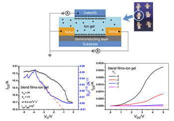
为了提高聚3-十二烷基噻吩的场效应迁移率, 将硅纳米线混入聚3-十二烷基噻吩的溶液中制成薄膜. 退火后的聚3-十二烷基噻吩能够自组装成有序的微晶结构, 有利于电子传输. 聚3-十二烷基噻吩薄膜在场效应晶体管中能够获得0.015 cm2·V-1·s-1的迁移率, 而混合薄膜能够获得高达0.68 cm2·V-1·s-1的迁移率. 这是因为硅纳米线优异的电子传输性能使得电子通过硅纳米线就像通过快速通道一样, 从而能够缩短电子在场效应晶体管中的传输时间, 提高传输速度. 此外, 使用离子胶作为介电层也能够提升场效应晶体管的性能, 混合薄膜能够获得高达6.2 cm2·V-1·s-1的迁移率.
朱昊云 , 黄威 , 黄宇立 , 汪伟志 . 硅纳米线和聚3-十二烷基噻吩混合薄膜在场效应晶体管中的应用研究[J]. 化学学报, 2016 , 74(5) : 429 -434 . DOI: 10.6023/A15120789
In order to enhance the field effect mobility of poly(3-dodecylthiophene), Si nanowires were added to the poly(3-dodecylthiophene) solution prior to film formation. The Si nanowires were produced by the electroless metal deposition method which involved the etching of silicon wafers in aqueous hydrofluoric acid and silver nitrate solution. The observation of scanning electron microscopy proved the uniform Si nanowires were obtained. The blend film was treated with thermal annealing to form ordered microcrystalline structure by self-organization. The annealing effect was measured by X-ray diffraction and atomic force microscopy which showed the enhancing diffraction peak and ordered atomic force microscopy images after annealing films. In the bottom gated field effect transistors, the blend film of Si nanowires and poly(3-dodecylthiophene) were formed on the SiO2/Si substrate by spin coating. The surface of the SiO2/Si substrate was coated with hexamethyldisilazane to produce a hydrophobic surface. The thickness of the Au source/drain electrodes was 100 nm. The annealing blend films worked as the semiconducting layer, 300 nm SiO2 worked as the gate dielectric and Si worked as the gate electrode. The charge carrier mobility of poly(3-dodecylthiophene) thin films was 0.015 cm2·V-1·s-1 and the charge carrier mobility of blend films was up to 0.68 cm2·V-1·s-1. The remarkable increase in the field effect mobility over that of pristine poly(3-dodecylthiophene) film is due to the high conductivity of Si nanowires which act as fast conducting channel between the crystalline regions of the poly(3-dodecylthiophene) film. To confirm and enhance the field effect transistors properties, we used the electric-double-layer transistor based on the blend films in which ion gel worked as the gate dielectric instead of SiO2. Here, Au foil worked as the gate electrode to form a top-gated field effect transistors. The charge carrier mobility of blend films was found to be relatively higher (6.2 cm2·V-1·s-1) when using ion gel as the dielectric layer.
[1] Padinger, F.; Rittberger, R. S.; Sariciftci, N. S. Adv. Funct. Mater. 2003, 13, 85.
[2] Li, G.; Shrotriya, V.; Huang, J.; Yao, Y.; Moriarty, T.; Emery, K.; Yang, Y. Nat. Mater. 2005, 4, 864.
[3] Jin, K. Y.; Lee, K.; Coates, N. E.; Daniel, M.; Nguyen, T.; Mark, D.; Heeger, A. J. Science 2007, 317, 222.
[4] He, M.; Han, W.; Ge, J.; Yu, W.; Yang, Y.; Qiu, F.; Lin, Z. Nanoscale 2011, 3, 3159.
[5] Pei, J.; Hao, Y.; Lü, H.; Sun, B.; Li, Y.; Wang, S. Acta Chim. Sinica 2014, 72(12), 1245. (裴娟, 郝彦忠, 吕海军, 孙宝, 李英品, 王尚鑫, 化学学报, 2014, 72(12), 1245.)
[6] Hao, Y.; Ma, J.; Sun, B.; Li, Y.; Ren, J. Acta Chim. Sinica 2010, 68(1), 33. (郝彦忠, 马洁霞, 孙宝, 李英品, 任聚杰, 化学学报, 2010, 68(1), 33.)
[7] Ohmori, Y.; Uchida, M.; Muro, K.; Yoshino, K. Jpn. Appl. Phys. 1991, 30, L1938.
[8] Ohmori, Y.; Uchida, M.; Muro, K.; Yoshino, K. Solid State Commun. 1991, 80, 605.
[9] Mcquade, D. T.; Pullen, A. E.; Swager, T. M. Chem. Rev. 2000, 100, 2537.
[10] Facchetti, A. Chem. Mater. 2011, 23, 733.
[11] Wang, C.; Dong, H.; Hu, W.; Liu, Y.; Zhu, D. Chem. Rev. 2012, 112, 2208.
[12] Zhao, G. J.; He, Y. J.; Peng, B. Chin. J. Chem. 2012, 30, 19.
[13] Scheinert, S.; Paasch, G.; Schrödner, M.; Roth, H. K.; Sensfuß, S.; Doll, T. J. Appl. Phys. 2002, 92, 330.
[14] Payerne, R.; Brun, M.; Rannou, P.; Baptist, R.; Grévin, B. Synth. Met. 2004, 146, 311.
[15] Tanaka, S.; Grévin, B.; Rannou, P.; Suzuki, H.; Mashiko, S. Thin Solid Films 2006, 499, 168.
[16] Sauvé, G.; Javier, A. E.; Zhang, R.; Liu, J.; Sydlik, S. A.; Kowalewski, T.; McCullough, R. D. J. Mater. Chem. 2010, 20, 3195.
[17] Babel, A.; Jenekhe, S. A. Synth. Met. 2005, 148, 169.
[18] Wang, G.; Swensen, J.; Moses, D.; Heeger, A. J. J. Appl. Phys. 2003, 93, 6137.
[19] Nagamatsu, S.; Takashima, W.; Kaneto, K.; Yoshida, Y.; Tanigaki, N.; Yase, K. Appl. Phys. Lett. 2004, 84, 4608.
[20] Yu, H. Z.; Peng, J. B. Acta Phys.-Chim. Sin. 2008, 24, 905. (於黄忠, 彭俊彪, 物理化学学报, 2008, 24, 905. )
[21] Motaung, D. E.; Malgas, G. F.; Nkosi, S. S.; Mhlongo, G. H.; Mwakikunga, B. W.; Malwela, T.; Arendse, C. J.; Muller, T. F. G.; Cummings, F. R. J. Mater. Sci. 2013, 48, 1763.
[22] Lu, G.; Tang, H.; Qu, Y.; Li, L.; Yang, X. Macromolecules 2007, 40, 6579.
[23] Babel, A.; Jenekhe, S. A. J. Phys. Chem. B 2003, 107, 1749.
[24] Zen, A.; Saphiannikova, M.; Neher, D.; Asawapirom, U.; Scherf, U. Chem. Mater. 2005, 17, 781.
[25] Jiu, T.; Reiss, P.; Guillerez, S.; Bettignies, R. D.; Bailly, S.; Chandezon, F. IEEE J. Sel. Top. Quant. 2010, 16, 1619.
[26] Kergoat, L.; Battaglini, N.; Miozzo, L.; Piro, B.; Pham, M. C.; Yassar, A.; Horowitz, G. Org. Electron. 2011, 12, 1253.
[27] Park, Y. D.; Lim, J. A.; Jang, Y.; Hwang, M.; Lee, H. S.; Lee, D. H.; Lee, H.; Baek, J.; Cho, K. Org. Electron. 2008, 9, 317.
[28] Tomioka, K.; Tanaka, T.; Hara, S.; Hiruma, K.; Fukui, T. IEEE J. Sel. Top. Quant. 2011, 17, 1112.
[29] Duan, X.; Niu, C.; Sahi, V.; Chen, J.; Parce, J. W.; Empedocles, S.; Goldman, J. L. Nature 2003, 425, 274.
[30] Chang, S.; Chuang, V. P.; Boles, S. T.; Ross, C. A.; Thompson, C. V. Adv. Funct. Mater. 2009, 19, 2495.
[31] Chen, Y. W.; Jiang, S. H.; Shao, B. X.; Wang, R. C. Chin. J. Inorg. Chem. 2007, 23, 915. (陈扬文, 江素华, 邵丙铣, 汪荣昌, 无机化学学报, 2007, 23, 915.)
[32] Yang, J. Y.; Lu, S. G.; Ding, H. Y.; Zhang, X. Y.; Kan, S. R. Chinese J. Inorg. Chem. 2010, 26, 1837. (杨娟玉, 卢世刚, 丁海洋, 张向军, 阚素荣, 无机化学学报, 2010, 26, 1837.)
[33] Srivastava, S. K.; Kumar, D.; Schmitt, S. W.; Sood, K. N.; Christiansen, S. H.; Singh, P. K. Nanotechnology 2014, 25, 175601.
[34] Peng, K.; Fang, H.; Hu, J.; Wu, Y.; Zhu, J.; Yan, Y.; Lee, S. Chem. Eur. J. 2006, 12, 7942.
[35] Liao, L.; Bai, J.; Lin, Y. C.; Qu, Y.; Huang, Y.; Duan, X. Adv. Mater. 2010, 22, 1941.
[36] Lei, T.; Dou, J.; Cao, X.; Wang, J.; Pei, J. Adv. Mater. 2013, 25, 6589.
[37] Fu, X. L.; Wang, C. L.; Li, R. J.; Dong, H. L.; Hu, W. P. Sci. China Chem. 2010, 6, 1225.
[38] Lin, J.; Zhong, J.; Zhong, S.; Li, H.; Zhang, H.; Chen, W. Appl. Phys. Lett. 2013, 103, 63109.
[39] Tarabella, G.; Mahvash Mohammadi, F.; Coppedè, N.; Barbero, F.; Iannotta, S.; Santato, C.; Cicoira, F. Chem. Sci. 2013, 4, 1395.
[40] Huang, J. K.; Jiang, P.; Hsu, C. L.; Chiu, M. H.; Juang, Z. Y.; Chang, Y. H.; Chang, W. H.; Iwasa, Y.; Takenobu, T.; Li, L. J. ACS Nano 2014, 8, 923.
[41] Yuan, H.; Shimotani, H.; Ye, J.; Yoon, S.; Aliah, H.; Tsukazaki, A.; Kawasaki, M.; Iwasa, Y. J. Am. Chem. Soc. 2010, 132, 18402.
[42] Zhang, J.; Han, Z.; Chen, M.; Yang, X.; Cao, W. J. Phys. Chem. Solids 2010, 71, 1316.
[43] Srivastava, S. K.; Kumar, D.; Schmitt, S. W.; Sood, K. N.; Christiansen, S. H.; Singh, P. K. Nanotechnology 2014, 25, 175601.
[44] Huang, J.; Pu, J.; Hsu, C.; Chiu, M.; Juang, Z.; Chang, Y.; Chang, W.; Iwasa, Y.; Takenobu, T.; Li, L. ACS Nano 2014, 8, 923.
/
| 〈 |
|
〉 |
