化学学报 ›› 2022, Vol. 80 ›› Issue (5): 581-589.DOI: 10.6023/A21120622 上一篇 下一篇
所属专题: 中国科学院青年创新促进会合辑
研究论文
何新蕊a,b, 蔡丽娜a,b, 陈汉生b, 尹攀b, 尹志刚b,c,*( ), 郑庆东b,*()
投稿日期:2021-12-31
发布日期:2022-05-31
通讯作者:
尹志刚, 郑庆东
作者简介:基金资助:
Xinrui Hea,b, Lina Caia,b, Hansheng Chenb, Pan Yinb, Zhigang Yinb,c(), Qingdong Zhengb()
Received:2021-12-31
Published:2022-05-31
Contact:
Zhigang Yin, Qingdong Zheng
About author:Supported by:文章分享

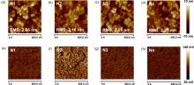
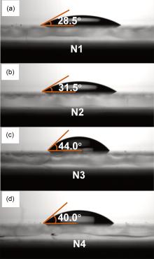
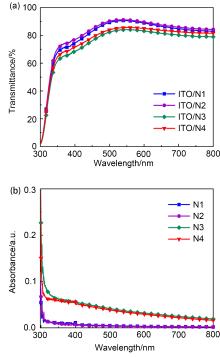
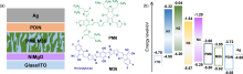
采用溶胶-凝胶法制备了Mg掺杂氧化镍(NiO)的三元氧化物半导体NiMgO薄膜, 研究了不同表面后处理方法对薄膜结构、性质和能级的影响. 利用NiMgO薄膜作为新型空穴传输界面层构建了非富勒烯有机太阳能电池, 研究了器件性能变化及其物理机制. 结果表明, 以未表面处理NiMgO为界面层时, 器件的能量转化效率(PCE)为5.90%; 使用紫外-臭氧(UVO)表面后处理的NiMgO界面层, 器件PCE大幅提升至12.67%. 而NiMgO在UVO处理前进行润洗, 可以去除表面残留物, 薄膜变平整且透光率增加. 因此, 采用润洗与UVO结合的表面双重后处理新策略后, 器件的开路电压不变, 但短路电流密度和填充因子分别提高到23.48 mA•cm–2和64.29%, 最终PCE达到13.17%. 该研究为半导体氧化物薄膜及器件的优化提供了一条有效途径.
何新蕊, 蔡丽娜, 陈汉生, 尹攀, 尹志刚, 郑庆东. 表面双重后处理方法提升三元NiMgO半导体界面层及其有机太阳能电池的性能※[J]. 化学学报, 2022, 80(5): 581-589.
Xinrui He, Lina Cai, Hansheng Chen, Pan Yin, Zhigang Yin, Qingdong Zheng. A Dual Post-Treatment Method for Improving the Performance of Ternary NiMgO Semiconductor Interfacial Layers and Their Organic Solar Cells※[J]. Acta Chimica Sinica, 2022, 80(5): 581-589.
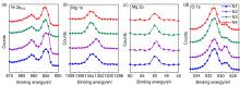


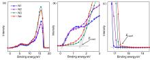
| NiMgO film | Eonset/eV | Ecutoff/eV | VBM/eV | CBM/eV | Ega/eV |
|---|---|---|---|---|---|
| N1 | 0.20 | 16.92 | –4.50 | –0.32 | 4.18 |
| N2 | 0.13 | 17.15 | –4.20 | –0.04 | 4.16 |
| N3 | 1.59 | 17.24 | –5.57 | –1.54 | 4.03 |
| N4 | 1.49 | 17.42 | –5.29 | –1.20 | 4.09 |
| NiMgO film | Eonset/eV | Ecutoff/eV | VBM/eV | CBM/eV | Ega/eV |
|---|---|---|---|---|---|
| N1 | 0.20 | 16.92 | –4.50 | –0.32 | 4.18 |
| N2 | 0.13 | 17.15 | –4.20 | –0.04 | 4.16 |
| N3 | 1.59 | 17.24 | –5.57 | –1.54 | 4.03 |
| N4 | 1.49 | 17.42 | –5.29 | –1.20 | 4.09 |


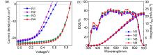

| NiMgO HTLs | VOC/V | JSC/(mA•cm–2) | FF/% | PCE/% | RSh/(kΩ•cm2) | RS/(Ω•cm2) | |
|---|---|---|---|---|---|---|---|
| Best | Avg. | ||||||
| N1 | 0.63 | 21.77 | 43.20 | 5.90 | 5.18 | 0.25 | 15.40 |
| N2 | 0.55 | 21.19 | 46.30 | 5.40 | 5.05 | 0.29 | 11.45 |
| N3 | 0.87 | 22.64 | 63.82 | 12.67 | 12.03 | 0.94 | 6.92 |
| N4 | 0.87 | 23.48 | 64.29 | 13.17 | 12.61 | 0.93 | 6.02 |


| [1] |
Wang, F.; Harindintwali, J. D.; Yuan, Z.; Wang, M.; Wang, F.; Li, S.; Yin, Z.; Huang, L.; Fu, Y.; Li, L.; Chang, S. X.; Zhang, L.; Rinklebe, J.; Yuan, Z.; Zhu, Q.; Xiang, L.; Tsang, D.; Xu, L.; Jiang, X.; Liu, J.; Wei, N.; Kästner, M.; Zou, Y.; Ok, Y. S.; Shen, J.; Peng, D.; Zhang, W.; Barceló, D.; Zhou, Y.; Bai, Z.; Li, B.; Zhang, B.; Wei, K.; Cao, H.; Tan, Z.; Zhao, L.; He, X.; Zheng, J.; Bolan, N.; Liu, X.; Huang, C.; Dietmann, S.; Luo, M.; Sun, N.; Gong, J.; Gong, Y.; Brahushi, F.; Zhang, T.; Xiao, C.; Li, X.; Chen, W.; Jiao, N.; Lehmann, J.; Zhu, Y.; Jin, H.; Schäffer, A.; Tiedje, J. M.; Chen, J. M. The Innovation 2021, 2, 100180.
doi: 10.1016/j.xinn.2021.100180 |
| [2] |
Classen, A.; Chochos, C. L.; Lüer, L.; Gregoriou, V. G.; Wortmann, J.; Osvet, A.; Forberich, K.; McCulloch, I.; Heumüller, T.; Brabec, C. J. Nat. Energy 2020, 5, 711.
doi: 10.1038/s41560-020-00684-7 |
| [3] |
Wang, W.; Wang, J.; Zheng, Z.; Hou, J. Acta Chim. Sinica 2020, 78, 382. (in Chinese)
doi: 10.6023/A20020032 |
|
(王文璇, 王建邱, 郑众, 侯剑辉, 化学学报, 2020, 78, 382.)
doi: 10.6023/A20020032 |
|
| [4] |
Lv, M.; Zhou, R.; Lv, K.; Wei, Z. Acta Chim. Sinica 2021, 79, 284. (in Chinese)
doi: 10.6023/A20090450 |
|
(吕敏, 周瑞敏, 吕琨, 魏志祥, 化学学报, 2021, 79, 284.)
doi: 10.6023/A20090450 |
|
| [5] |
Guo, X.; Cui, C.; Zhang, M.; Huo, L.; Huang, Y.; Hou, J.; Li, Y. Energy Environ. Sci. 2012, 5, 7943.
doi: 10.1039/c2ee21481d |
| [6] |
Yu, G.; Gao, J.; Hummelen, J. C.; Wudi, F.; Heeger, A. J. Science 1995, 270, 1789.
doi: 10.1126/science.270.5243.1789 |
| [7] |
Yin, Z.; Zheng, Q.; Chen, S.; Cai, D.; Ma, Y. Adv. Energy Mater. 2016, 6, 1501493.
|
| [8] |
Yin, Z.; Wei, J.; Chen, S.; Cai, D.; Ma, Y.; Wang, M.; Zheng, Q. J. Mater. Chem. A 2017, 5, 3888.
doi: 10.1039/C6TA10981K |
| [9] |
Zhao, J.; Li, Y.; Yang, G.; Jiang, K.; Lin, H.; Ade, H.; Ma, W.; Yan, H. Nat. Energy 2016, 1, 15027
doi: 10.1038/nenergy.2015.27 |
| [10] |
Lin, Y.; Wang, J.; Zhang, Z.; Bai, H.; Li, Y.; Zhu, D.; Zhan, X. Adv. Mater. 2015, 27, 1170.
doi: 10.1002/adma.201404317 |
| [11] |
Li, T.; Zhan, X. Acta Chim. Sinica 2021, 79, 257. (in Chinese)
doi: 10.6023/A20110502 |
|
(李腾飞, 占肖卫, 化学学报, 2021, 79, 257.)
doi: 10.6023/A20110502 |
|
| [12] |
Zhang, J.; Tan, H.; Guo, X.; Facchetti, A.; Yan, H. Nat. Energy 2018, 3, 720.
doi: 10.1038/s41560-018-0181-5 |
| [13] |
Yuan, J.; Zhang, Y.; Zhou, L.; Zhang, G.; Yip, H.; Lau, T.; Lu, X.; Zhu, C.; Peng, H.; Johnson, P. A.; Leclerc, M.; Cao, Y.; Ulanski, J.; Li, Y.; Zou, Y. Joule 2019, 3, 1140.
doi: 10.1016/j.joule.2019.01.004 |
| [14] |
Li, C.; Zhou, J.; Song, J.; Xu, J.; Zhang, H.; Zhang, X.; Guo, J.; Zhu, L.; Wei, D.; Han, G.; Min, J.; Zhang, Y.; Xie, Z.; Yi, Y.; Yan, H.; Gao, F.; Liu, F.; Sun, Y. Nat. Energy 2021, 6, 605.
doi: 10.1038/s41560-021-00820-x |
| [15] |
Ma, Y.; Cai, D.; Wan, S.; Yin, P.; Wang, P.; Lin, W.; Zheng, Q. Natl. Sci. Rev. 2020, 7, 1886.
doi: 10.1093/nsr/nwaa189 |
| [16] |
Tang, C.; Ma, X.; Wang, J.; Zhang, X.; Liao, R.; Ma, Y.; Wang, P.; Wang, P.; Wang, T.; Zhang, F.; Zheng, Q. Angew. Chem., Int. Ed. 2021, 60, 19314.
doi: 10.1002/anie.202105861 |
| [17] |
Liu, Y.; Liu, B.; Ma, C.; Huang, F.; Feng, G.; Chen, H.; Hou, J.; Yan, L.; Wei, Q.; Luo, Q.; Bao, Q.; Ma, W.; Liu, W.; Li, W.; Wan, X.; Hu, X.; Han, Y.; Li, Y.; Zhou, Y.; Zou, Y.; Chen, Y.; Li, Y.; Chen, Y.; Tang, Z.; Hu, Z.; Zhang, Z.; Bo, Z. Sci. China: Chem. 2022, 65, 224.
|
| [18] |
Yin, Z.; Wei, J.; Zheng, Q. Adv. Sci. 2016, 3, 1500362.
|
| [19] |
Ma, C.; Fu, W.; Huang, G.; Chen, H.; Xu, M. Acta Chim. Sinica 2015, 73, 949. (in Chinese)
doi: 10.6023/A15040246 |
|
(马春燕, 傅伟飞, 黄国伟, 陈红征, 徐明生, 化学学报, 2015, 73, 949.)
doi: 10.6023/A15040246 |
|
| [20] |
Guang, S.; Yu, J.; Wang, H.; Liu, X.; Qu, S.; Zhu, R.; Tang, W. J. Energy Chem. 2021, 56, 496.
|
| [21] |
Zhang, C.; Luo, Q.; Wu, H.; Li, H.; Lai, J.; Ji, G.; Yan, L.; Wang, X.; Zhang, D.; Lin, J.; Chen, L.; Yang, J.; Ma, C. Org. Electron. 2017, 45, 190.
doi: 10.1016/j.orgel.2017.03.015 |
| [22] |
Yip, H.; Jen, A. Energy Environ. Sci. 2012, 5, 5994.
doi: 10.1039/c2ee02806a |
| [23] |
Liu, J.; Xue, Y.; Gao, Y.; Yu, D.; Durstock, M.; Dai, L. Adv. Mater. 2012, 24, 2228.
doi: 10.1002/adma.201104945 |
| [24] |
Yin, Z.; Zheng, Q.; Chen, S.; Cai, D. ACS Appl. Mater. Interfaces 2013, 5, 9015.
doi: 10.1021/am402175m |
| [25] |
Lou, Y. H.; Wang, Z. K. Nanoscale 2017, 9, 13506.
doi: 10.1039/C7NR04692H |
| [26] |
Zhan, T.; Ren, P.; Huang, X.; Zhang, X.; Chen, G.; Xiong, J.; Xue, X.; Cai, P.; Zhang, J.; Chen, J. Solar Energy 2021, 216, 211.
doi: 10.1016/j.solener.2021.01.037 |
| [27] |
Manders, J. R.; Tsang, S.; Hartel, H. J.; Lai, T.; Chen, S.; Amb, C. M.; Reynolds, J. R.; So, F. Adv. Funct. Mater. 2013, 23, 2993.
doi: 10.1002/adfm.201202269 |
| [28] |
Jiang, F.; Choy, W. C. H.; Li, X.; Zhang, D.; Cheng, J. Adv. Mater. 2015, 27, 2930.
doi: 10.1002/adma.201405391 |
| [29] |
Hossain, M. A.; Zhang, T.; Zakaria, Y.; Lambert, D.; Burr, P. A.; Rashkeev, S. N.; Abdallah, A.; Hoex, B. IEEE J. Photovolt. 2021, 11, 1176.
doi: 10.1109/JPHOTOV.2021.3095458 |
| [30] |
Zhang, J. Y.; Li, W. W.; Hoye, R. L. Z.; Macmanus-Driscoll, J. L.; Budde, M.; Bierwagen, O.; Wang, L.; Du, Y.; Wahila, M. J.; Piper, L. F. J.; Lee, T. L.; Edwards, H. J.; Dhanak, V. R.; Zhang, K. H. L. J. Mater. Chem. C 2018, 6, 2275.
doi: 10.1039/C7TC05331B |
| [31] |
Denny, Y. R.; Lee, K.; Park, C.; Oh, S. K.; Kang, H. J.; Yang, D.; Seo, S. Thin Solid Films 2015, 591, 255.
doi: 10.1016/j.tsf.2015.04.043 |
| [32] |
Wang, N.; Liu, C. Q.; Wen, C. Q. L. B.; Wang, H. L.; Liu, S. M.; Jiang, W. W.; Ding, W. Y.; Chai, W. P. Thin Solid Films 2016, 616, 587.
doi: 10.1016/j.tsf.2016.08.051 |
| [33] |
Huang, S.; Wang, Y.; Shen, S.; Tang, Y.; Yu, A.; Kang, B.; Silva, S. R. P.; Lu, G. J. Colloid Interface Sci. 2019, 535, 308.
doi: 10.1016/j.jcis.2018.10.013 |
| [34] |
Mares, J. W.; Boutwell, C. R.; Scheurer, A.; Falanga, M.; Schoenfeld, W. V. Proc. SPIE 2010, 7603, 76031B.
|
| [35] |
Yin, Z.; Zheng, Q.; Chen, S.; Cai, D.; Zhou, L.; Zhang, J. Adv. Energy Mater. 2014, 4, 1301404.
|
| [36] |
Zhai, Z.; Huang, X.; Xu, M.; Yuan, J.; Peng, J.; Ma, W. Adv. Energy Mater. 2013, 3, 1614.
doi: 10.1002/aenm.201300272 |
| [1] | 张璇, 熊军, 张旺. 通过聚(3,4-乙烯二氧噻吩)-聚苯乙烯磺酸改性实现高性能蓝色钙钛矿发光二极管[J]. 化学学报, 2023, 81(12): 1695-1700. |
| [2] | 白阳, 薛灵伟, 王海侨, 张志国. 苯并三氮唑类有机光伏材料研究进展[J]. 化学学报, 2021, 79(7): 820-852. |
| [3] | 马春燕, 傅伟飞, 黄国伟, 陈红征, 徐明生. 高性能的二维层状材料硫化钨界面层的有机太阳能电池[J]. 化学学报, 2015, 73(9): 949-953. |
| [4] | 薛启帆, 孙辰, 胡志诚, 黄飞, 叶轩立, 曹镛. 钙钛矿太阳电池研究进展:薄膜形貌控制与界面工程[J]. 化学学报, 2015, 73(3): 179-192. |
| [5] | 付钰, 王芳, 张燕, 方旭, 赖文勇, 黄维. 非富勒烯小分子有机太阳能电池电子受体材料的研究进展[J]. 化学学报, 2014, 72(2): 158-170. |
| [6] | 杨家义,史铁钧,金维亚,邹燕. 对氨基苯磺酸两步法修饰多壁碳纳米管[J]. 化学学报, 2008, 66(5): 552-556. |
| [7] | 金毅亮 秦 维 蒋 芸 王 梅. 金银合金纳米粒子表面处理及其表面增强拉曼光谱研究[J]. 化学学报, 2008, 66(22): 2494-2498. |
| [8] | 雷景新, 何光健, 高峻. CaCO3粉末表面光聚合处理的研究[J]. 化学学报, 2004, 62(5): 523-526. |
| [9] | 岳林海,谢伟宏,水淼,徐铸德. 聚丙烯酸包覆超细碳酸钙的机理和表面性质研究[J]. 化学学报, 2002, 60(7): 1156-1161. |
| 阅读次数 | ||||||
|
全文 |
|
|||||
|
摘要 |
|
|||||
